
Amplifier Circuit
Index 115
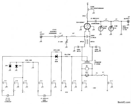
6_METER_KILOWATT_AMPLIFIER
Published:2009/7/6 4:54:00 Author:May
Circuit Notes
The amplifier uses a grounded grid circuit with either the Eimac 3CX1000A7 or 8877, ceramic/metal triodes intended for linear service in the HP and VHF ranges. The amp provides the legal power output of 1500 watts PEP and CW service with no effort and requires a driver delivering between 50 and 80 watts at 50 MHz. With a plate voltage of 3000 volts at 0.8 amps the amplifier performs at 60 percent efficiency. The grid is grounded by means of the grid ring of the 3CX1000A7 socket providing a lowinductance path to ground. The amplifier is completely stable. (View)
View full Circuit Diagram | Comments | Reading(3569)
LOW_POWER_COMMON_SOURCE_AMPLIFIER
Published:2009/7/6 4:47:00 Author:May
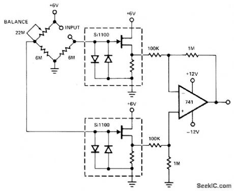
A circuit that will operate in the 10- to 20- microamp range at a 12-volt supply voltage. The diode protection is available in this configuration. The circuit voltage gain will be between 10 and 20, with extremely low power consumption (approximately 250 μW).This is very desirable for remote or battery operation where minimum maintenance is important. (View)
View full Circuit Diagram | Comments | Reading(844)
TYPICAL_TWO_OP_AMP_BRIDGE_TYPE_DIFFERENTIAL_AMPLIFIER
Published:2009/7/6 4:44:00 Author:May
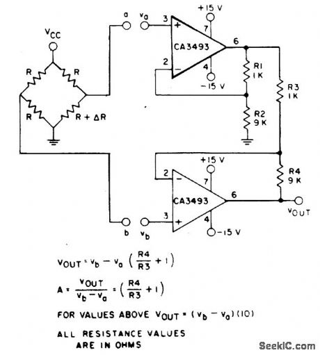
Using a CA3493 BiMOS op amp to provide high input impedance and good common-mode rejection ratio (depends primarily on matching of resistor networks). (View)
View full Circuit Diagram | Comments | Reading(584)
Video_line_driving_amplifier
Published:2009/7/23 20:20:00 Author:Jessie
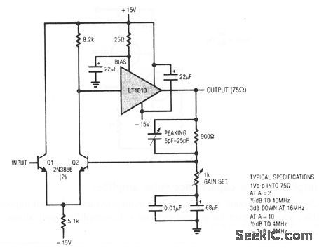
This circuit combines the LT1010's load-handling capability with a fast, discrete gain stage. Q1 and Q2 form a differential stage that single-ends into the LT1010. For video applications that are sensitive to NTSC requirements, dropping the bias resistor will aid performance. The peaking adjustment should be optimized under loaded output conditions. (View)
View full Circuit Diagram | Comments | Reading(0)
Minimum_component_bridge_amplifier
Published:2009/7/23 20:11:00 Author:Jessie
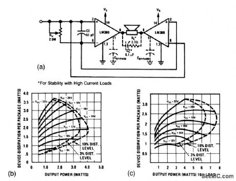
This circuit shows two LM380 ICs connected to double the audiooutput power of a single LM380.The Circuit provides twice the voltage swing across the load for a given supply, increasing the power capability by a factor of four over the single amplifier. However, in most cases, the package dissipation is the first parameter that limits power to the load. In such cases, the power capability of the bridge circuit is only twice that of the single IC. Figures 1-37B and 1-37C show output power versus device-package dissipation for both 8- and 16-Ω loads in the bridge configuration. Notice that the 3% and 10% harmonic distortion contours double back (because of the thermal limiting of the LM380). Different amounts of heatsinking will change the point at which the distortion contours bend. (View)
View full Circuit Diagram | Comments | Reading(788)
Linearized_platinum_resistance_thermometer
Published:2009/7/23 20:06:00 Author:Jessie
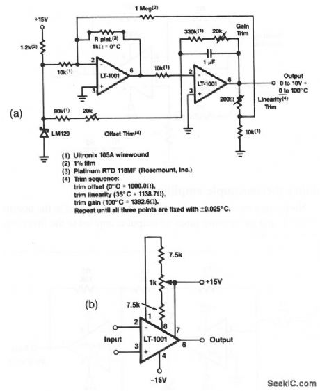
With the values shown, this circuit has a ±0.025°C accuracy over 0° to 100°C. The input offset voltage of the LT-1001, and its drift with temperature, are permanently trimmed at wafer test to a low level. However, if further adjustment of VOS is necessary, nulling with the circuit of Fig. 10-4B will not degrade drift with temperature. The Fig. 10-4B offset circuit has an approximate null range of ±100 μV. o Raytheon U near Integrated a rcuts 1989, p. 4-45. (View)
View full Circuit Diagram | Comments | Reading(713)
TOTEM-POLE_DRIVER_WITH_BOOTSTRAPPING
Published:2009/7/6 4:23:00 Author:May

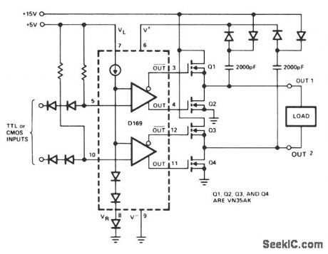
When driving MOSPOWER in a totem-pole output conftguration, it is necessary to have the gate voltage 10 to 15 V positive with respect to the source in order to handle load currents near the MOSPOWER maximum ratings. The D169 lends itself to bootstrapping because of its high-voltage ratings. In the circuit shown, the voltage on the 2000-pF bootstrap capacitors is applied via diode OR gates to the V+ terminal. Therefore, regardless of which output is high, 30 V is present at V +.Maximum switching frequency is determined by the input capacitance of the MOSPOWER transistors used. (View)
View full Circuit Diagram | Comments | Reading(1840)
BASIC_PNPN_MEMORY
Published:2009/7/23 2:10:00 Author:Jessie
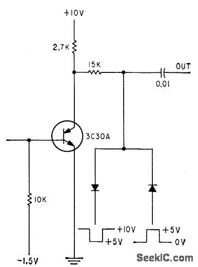
Delivers either positive or negative pulse output, accomplished by means of coupling diodes and transition memory capacitor.-J. B. Hangstefer and L. H. Dixon, Jr., Triggered Bistable Semiconductor Circuits, Electronics, 32:35, p 58-60. (View)
View full Circuit Diagram | Comments | Reading(659)
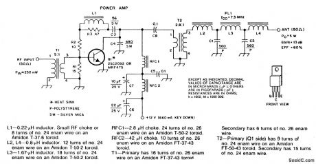
125_WATT_150_MHz_AMPLIFIER
Published:2009/7/6 4:22:00 Author:May
Circuit Notes
This amplifier operates from a 28 Vdc supply. It has a typical gain of 12 dB, and can survive operation into a 30:1 VSWR load at any phase angle with no damage. The amplifier has an AGO range in excess of 20 dB. This means that with input power held constant at the level that provides 125 watts output, the output power may be reduced to less than 1.0 watt continuously by driving the dc gate voltage negative from its IDQ value. (View)
View full Circuit Diagram | Comments | Reading(726)
AF_SINE_SQUARE_TRIANGLE
Published:2009/7/6 4:21:00 Author:May
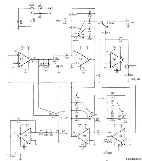
Can be tuned over entire audio spectrum in four ranges for generation of low-distortion waves for laboratory use. IC1 converts sine wave to square wave. IC3 acts as integrator converting squarewave output of IC1 to triangle wave. IC4-IC6 form statevariable filter for removing sinewave componentfrom triangle wave. IC2 is simple inverting amplifier for output.-R.Melenand H. Garland,″Understanding lC Operational Amplifiers,″Howard W.Sams,Indianapolis,IN,2nd Ed.,1978,p 130-134.
(View)
View full Circuit Diagram | Comments | Reading(1049)
6_METER_PREAMPLIFIER_PROVIDES_20_dB_GAIN_AND_LOW_NF
Published:2009/7/6 4:19:00 Author:May
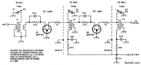
Circuit NotesC1, C2, and C3 are miniature ceramic or plastic trimmers. T1 (main winding) is 0.34μH. Use of 11 turns of no. 24 enameled wire on a T37-10 toroid core. The antenna winding has one turn, and Q1 the source winding has three turns. T2 primary consists of 11 turns of no. 24 enameled wire on a T37-10 toroid. Tap Q1 drain is three turns from C2 the end of the winding. The secondary has three turns. T3 is the same as T2, except its secondary has one turn. (View)
View full Circuit Diagram | Comments | Reading(705)
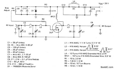
5_W_RF_POWER_AMPLIFIER
Published:2009/7/6 4:13:00 Author:May
Circuit NotesNumbered components are so designated for PC-board layout purposes. C5 and C8 are disc ceramic. C6 and C7 are tantalum or electrolytic. R1, R2 and R3 are 1/2W carbon composition resistors. Silver-mica capacitors may be substituted for polystyrene (P) types. Impedance transformation ratios are shown above T1 and T2. (View)
View full Circuit Diagram | Comments | Reading(962)
1_WATT,23_GHz_AMPLIFIER
Published:2009/7/6 4:07:00 Author:May

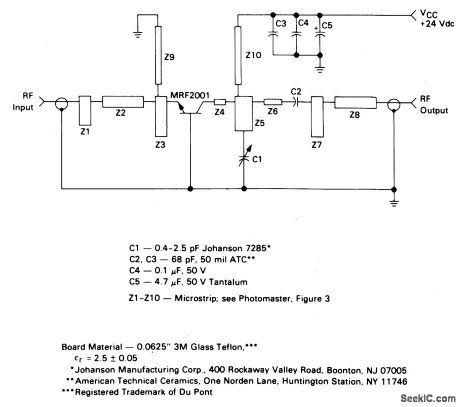
Circuit Notes
Simplicity and repeatability are feature-d in this 1 watt S-band amplifier design. The design uses an MRF2001 transistor as a common base, Class C amplifier. The amplifier delivers 1 watt output with 8 dB minimum gain at 24 V, and is tunable from 2.25 to 2.35 GHz. Applications include microwave communications equipment and other systems requiring medium power, narrow band amplification. The amplifier circuitry consists almost entirely of distributed microstrip elements. A total of six additional components, including the MRF2001, are required to build a working amplifier. The input and output impedances of the transistor are matched to 50 ohms by double section low pass networks. The networks are designed to provide about 3% 1 dB power bandwidth while maintaining a collector efficiency of approximately 30%. There is one tuning adjustment in the amplifier-C1 in the output network. Ceramic chip capacitors, C2 and C3, are used for dc blocking and power supply decoupling. Additional low frequency decoupling is provided by capacitors C4 and C5. (View)
View full Circuit Diagram | Comments | Reading(730)
LOW_DISTORTION_16_TO_30_MHz_SSB_DRIVER
Published:2009/7/6 3:57:00 Author:May
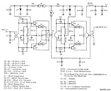
Circuit Notes
The amplifier provides a total power gain of about 25 dB, and the construction technique allows the use of inexpensive components throughout. The MRF476 is specified as a 3 watt device and the MRF475 has an output power of 12 watts. Both are extremely tolerant to overdrive and load mismatches, even under CW conditions. Typical IMD numbers are better than -35 dB, and the power gains are 18 dB and 12 dB, respectively, at 30 MHz. The bias currents of each stage are individually adjustable with R5 and R6. Capacitors C4 and CIO function as audio-frequency bypasses to further reduce the source impedance at the frequencies of modulation. Gain leveling across the band is achieved with simple RC networks in series with the bases, in conjunction with negative feedback. The amplitude of the out-of-phase voltages at the bases is inversely proportional to the frequency as a result of the series inductance in the feedback loop and the increasing input impedance of the transistor at low frequencies. Conversely, the negative feedback lowers the effective input impedance presented to the source (not the input impedance of the device itself) and with proper voltage slope would equalize it. With this technique, it is possible to, maintain an input VSWR of 1.5:1 or less than 1.6 to 30 MHz. (View)
View full Circuit Diagram | Comments | Reading(782)
High_impedance_low_capacitance_video_amplifier
Published:2009/7/23 20:17:00 Author:Jessie
This compound series-feedback circuit provides high input impedance and stable, wideband gain for general-purpose video-amplifier applications. (View)
View full Circuit Diagram | Comments | Reading(695)
Voltage_controlled_variable_gain_video_amplifier
Published:2009/7/23 20:15:00 Author:Jessie
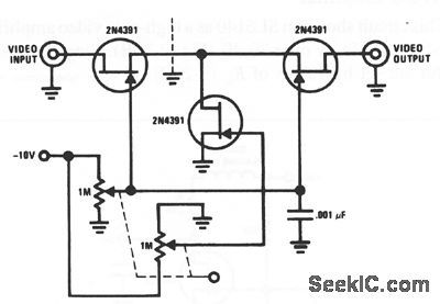
The 2N4391 provides a low RDS(ON) (less than 30Ω). The tee attenuator provides for optimum dynamic linear range for attenuation. If complete turnoff is desired, attenuation of greater than 100 dB can be obtained at 10 MHz, provided that proper RF-construction techniques are used (proper shielding to prevent input passing to output around the FETs). (View)
View full Circuit Diagram | Comments | Reading(1442)
Photodiode_amplifier
Published:2009/7/23 20:14:00 Author:Jessie
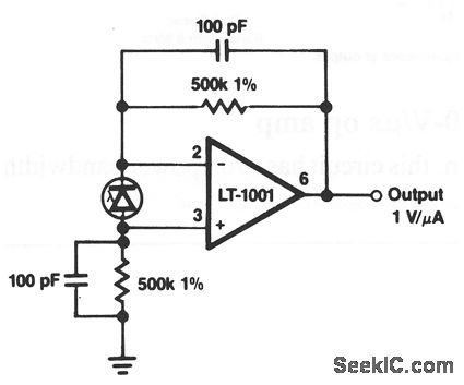
This circuit produces a 1-Voutput for a 1-μA input. (View)
View full Circuit Diagram | Comments | Reading(0)
Wideband_AGC_amplifier
Published:2009/7/23 20:13:00 Author:Jessie
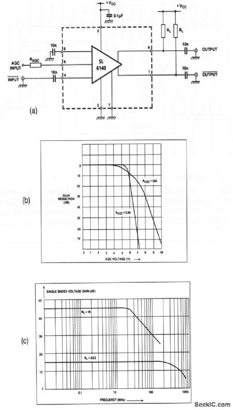
This circuit shows an SL6140 as a high-gain video amplifier, with AGC capable of reducing gain by over 70 dB (Fig. 3-20B). Single-ended voltage gain and bandwidth are set by values of RL (3-20C). (View)
View full Circuit Diagram | Comments | Reading(0)
Microvolt_comparator_with_TTL_output
Published:2009/7/23 20:12:00 Author:Jessie
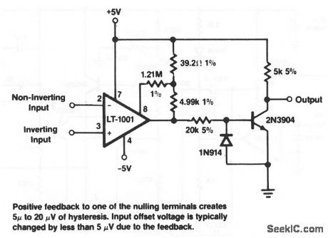
This circuit produces a full 5-V TTL output with microvolt (differential )inputs. (View)
View full Circuit Diagram | Comments | Reading(751)
90_W_audio_power_amplifier
Published:2009/7/23 20:36:00 Author:Jessie
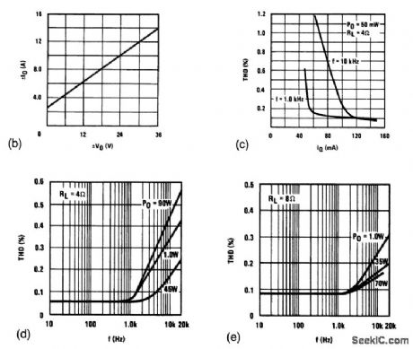
This circuit is capable of 90 W into a 4-Ω speaker, or 70 W into an 8-Ω speaker. The circuit features safe area, short-circuit and overload protection, harmonic distortion less than 0.1% at 1.0 kHz, and an all-npn output stage. Figures 1-42B through 1-42E show the circuit performance characteristics. (View)
View full Circuit Diagram | Comments | Reading(1148)
| Pages:115/250 At 20101102103104105106107108109110111112113114115116117118119120Under 20 |
Circuit Categories
power supply circuit
Amplifier Circuit
Basic Circuit
LED and Light Circuit
Sensor Circuit
Signal Processing
Electrical Equipment Circuit
Control Circuit
Remote Control Circuit
A/D-D/A Converter Circuit
Audio Circuit
Measuring and Test Circuit
Communication Circuit
Computer-Related Circuit
555 Circuit
Automotive Circuit
Repairing Circuit