
Amplifier Circuit
Index 120
Ac_coupled_inverting_amplifier
Published:2009/7/23 21:41:00 Author:Jessie
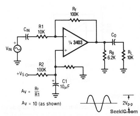
This circuit is the ac versionof the basic dc circuit in Fig. 10-26. (View)
View full Circuit Diagram | Comments | Reading(790)
Ac_coupled_noninverting_amplifier
Published:2009/7/23 21:41:00 Author:Jessie
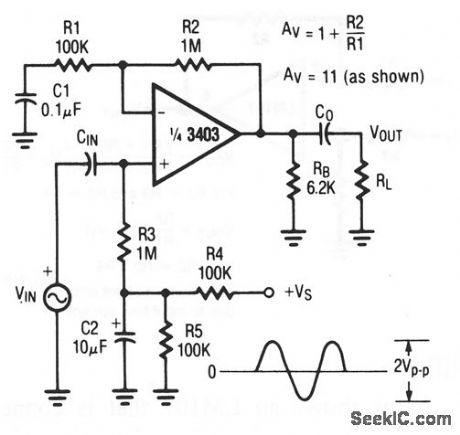
This circuit is the ac version of the basic dc circuit in Fig. 10-27. (View)
View full Circuit Diagram | Comments | Reading(871)
High_level_mixer
Published:2009/7/23 21:40:00 Author:Jessie
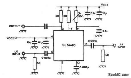
The SL6440,shown is a double-balanced mixer, for use in RF systems up to 150 MHz. External selection of the dc operating conditions is controlled by the resistor connected between pin 11 (bias) and VCC. Conversion gain for single-ended circuit of Fig. 2-10 is equal to: GdB 20 Log56.61+0.0785,RLIp, where Ip is programmed current at pin 11, and RL is dc load resistance. (View)
View full Circuit Diagram | Comments | Reading(1148)
Single_chip_audio_amplifier_BTL_015W
Published:2009/7/23 23:55:00 Author:Jessie
This circuit make use of the bridge-tied load (BTL) principle to achieve low-voltage operation without sacrifice of output power ,The circuit operates with battery supplies from 6V down to 1.6V ,and draws low quiescent current (typically 3.2mA with 3-V supply).Closed-loop voltage gain is 32dB with connections, as shown (floating differential input ,3-Vsupply and 32-Ω load).Output is reduced to 0.14 when supply is reduced to 3V (with 32-Ω load). (View)
View full Circuit Diagram | Comments | Reading(1061)
125_W_150_MHz_TMOS_FET_amplifier
Published:2009/7/23 22:59:00 Author:Jessie
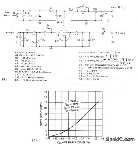
This circuit uses an MRF174 TMOS FET, has a typical gain of 12 dB, and can survive operation into a 30:1 VSWR load at any phase angle with no damage. Notice that the output power can be reduced to loss than 1W continuously by driving the dc gate voltage negative (by adjusting R3). Figure 2-53B shows this performance feature. (View)
View full Circuit Diagram | Comments | Reading(997)
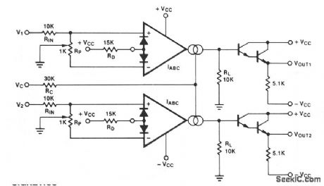
Differential_input_instrumentation_amplifier
Published:2009/7/23 21:45:00 Author:Jessie

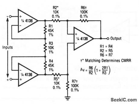
This circuit uses three sections of a 4136 to form an instrumentation amplifier, where the common-mode rejection ratio depends on the matching of resistors. (View)
View full Circuit Diagram | Comments | Reading(1730)
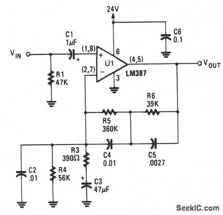
High_impedance_differential_amplifier
Published:2009/7/23 21:44:00 Author:Jessie
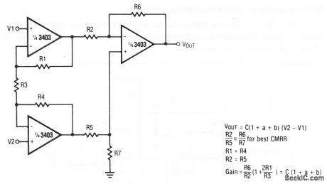
This circuit uses three sections of a 3404 op amp to form a high-impedance amplifier, where the output depends on the difference between V1 and V2, as well as the resistance ratios. By eliminating the input resistances (such as shown in Fig. 10-29), input impedance depends on the 3404 alone.
(View)
View full Circuit Diagram | Comments | Reading(0)
AC-Coupled Differential Amplification Principle Circuit
Published:2011/7/27 8:43:00 Author:Robert | Keyword: AC-Coupled, Differential, Amplification, Principle
The picture shows the AC-coupled differential amplification principle circuit. (View)
View full Circuit Diagram | Comments | Reading(2519)
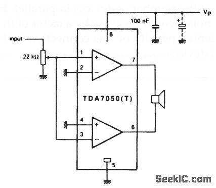
MAGNETIC_PHONO_PREAMPLIFIER
Published:2009/7/5 23:53:00 Author:May
View full Circuit Diagram | Comments | Reading(0)
Programmable Gain Buffer Amplification Circuit With Super Use Of Floating Exchange
Published:2011/7/30 19:41:00 Author:Robert | Keyword: Programmable, Gain, Buffer, Amplification, Super, Use, Floating Exchange
The picture shows the programmable gain buffer amplification circuit with super use of floating exchange. (View)
View full Circuit Diagram | Comments | Reading(511)
LINE_OPERATED_AMPLIFIER
Published:2009/7/5 23:52:00 Author:May
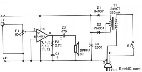
T1 isolates the unit from the line, and has a 24-V, center-tapped secondary. The output of the transformer is rectified by diodes D1 and D2 and filtered by capacitor C3 to provide 15 to 18 Vdc. The LM383 has built-in protection against speaker shorts. (View)
View full Circuit Diagram | Comments | Reading(1703)
1_A_LAMP_FLASHER
Published:2009/7/5 23:52:00 Author:May
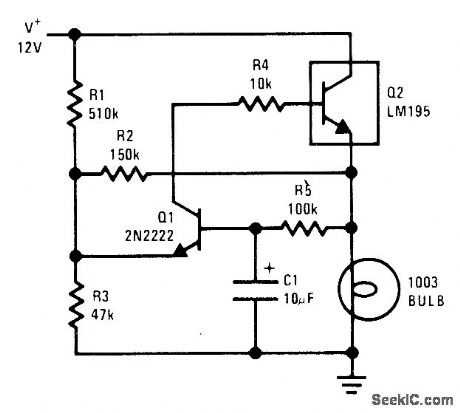
National LM195 power transistor is turned on and off once per second for flashing 12-V lamp. Current limiting in LM195 prevents high peak currents during turnon even though cold lamp can draw 8 times normal operating current. Current-limiting feature prolongs lamp life in flashing applications.-R.Dobkin, Fast IC Power Transistor with Thermal Protection, National Semiconductor, Santa Clara, CA, 1974, AN-110, p 5. (View)
View full Circuit Diagram | Comments | Reading(821)
AUDIO_AMPLIFIER
Published:2009/7/5 23:47:00 Author:May
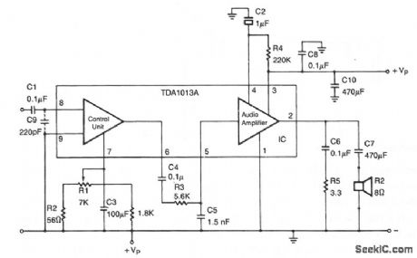
C9 is necessary to filter-out rf input interferences.R3 in combination with C5 is used to limit the af frequency bandwidth.The 470-μF power supply decoupling capacitor is C10. (View)
View full Circuit Diagram | Comments | Reading(2363)
A Gain-Program-Control Apparatus Amplification Circuit
Published:2011/7/27 3:28:00 Author:Robert | Keyword: Gain, Program, Control, Apparatus, Amplification
The picture shows thea gain-program-control apparatus amplification circuit. (View)
View full Circuit Diagram | Comments | Reading(598)
MICRO_SIZED_AMPLIFIER
Published:2009/7/5 23:43:00 Author:May
Sound detected by electret microphone MIC1 is fed to IC1's input through resistor R2, and capacitors C1 and C2. Resistors R2 and R5 determine the overall stage gain, while C2 partially determines the amplifier's frequency response. To ensure proper operation, use a single-ended power supply. R3 and R4 simulate a null condition equal to half the power supply's voltage at IC1's noninverting input. The output of IC1 is transferred to emitter-follower amplifier Q1 via volume control R6. The high-Z-in/low-Z-out characteristic of the emitter-follower matches the moderately high-impedance output of IC1 to a low-impedance headphone load. (View)
View full Circuit Diagram | Comments | Reading(706)
Double_conversion_IF_strip
Published:2009/7/23 22:01:00 Author:Jessie
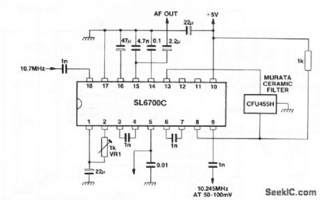
This circuit shows an SL6700 (Fig. 2-13) connected to form a double-conversion (10.7 MHz and 455 kHz) IF strip, using a ceramic filter for the 455-kHz network. The sensitivity of this circuit is typically 5μV (rms), with 30% modulation for a 10-dB S/N ratio. The circuit will accept up to 100 mV (rms) at 80% modulation with distortion below 5%. (View)
View full Circuit Diagram | Comments | Reading(2463)
POSITIVE_LOGIC_LAMP_DRIVER
Published:2009/7/23 21:54:00 Author:Jessie
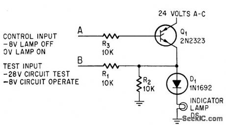
Turns on lamp for zero or positive control pulse at A. Negative pulse at B tests condition of circuit and lamp.-A. E. Popodi, Reliable Repertoire Of Display Circuits, Electronics, 38:2, p 60-66. (View)
View full Circuit Diagram | Comments | Reading(651)
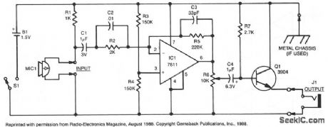
MICROPHONE_AMPLIFIER
Published:2009/7/5 23:14:00 Author:May
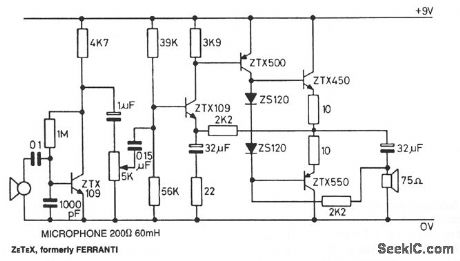
This circuit features the ZTX450/ZTX550 transistors in a push-pull output stage. The following read-ings were taken at maximum volume:
Input:O.4mVrms Output:l.8Vrms Voltage gain:4500Max. output before distortion: 2.25 V rms- supply current = 3.5 mA Zero output-supply current: 3.5 mAWattage:0.034 WFrequency response: 250 Hz to 28 kH (View)
View full Circuit Diagram | Comments | Reading(0)
GAIN_CONTROLLED_STEREO_AMPLIFIER
Published:2009/7/5 23:13:00 Author:May
View full Circuit Diagram | Comments | Reading(596)
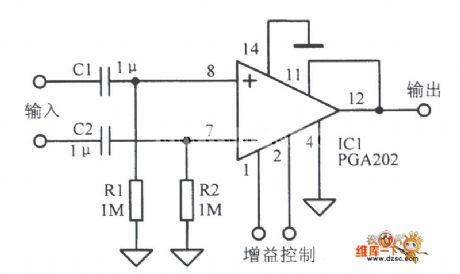
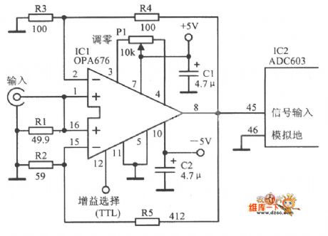
Floating Signal Source Programmable Gain Amplifier Circuit Composed Of PGA203
Published:2011/7/29 9:10:00 Author:Robert | Keyword: Floating, Signal, Source, Programmable, Gain, Amplifier
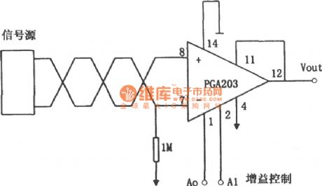
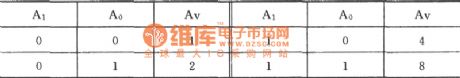
The picture shows the floating signal source programmable gain amplifier circuit. This circuit uses digital-control instrumentation amplifier PGA203 integrated chip. Its programmable gain have: 1, 2, 4, 8 (binary). It has low bias current (maximum value is 50pA) and fast setup time (2us can be 0.01%) and low nonlinear distortion (maximum nonlinear distortion is 0.012%) and high CMRR (minimum value is 80dB).
The relations between the control ports A0, A1's voltage level and the gain Av is listed in picture 2. (View)
View full Circuit Diagram | Comments | Reading(647)
| Pages:120/250 At 20101102103104105106107108109110111112113114115116117118119120Under 20 |
Circuit Categories
power supply circuit
Amplifier Circuit
Basic Circuit
LED and Light Circuit
Sensor Circuit
Signal Processing
Electrical Equipment Circuit
Control Circuit
Remote Control Circuit
A/D-D/A Converter Circuit
Audio Circuit
Measuring and Test Circuit
Communication Circuit
Computer-Related Circuit
555 Circuit
Automotive Circuit
Repairing Circuit