
Amplifier Circuit
Index 121
Multi-Stage Output Delay Circuit
Published:2011/7/27 8:41:00 Author:Robert | Keyword: Multi-Stage, Output, Delay
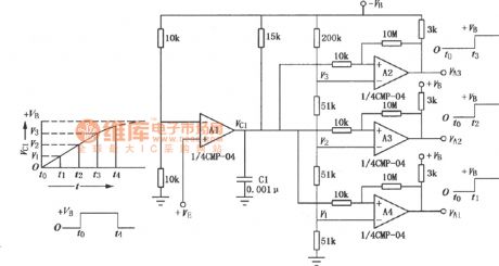
The picture shows the multi-stage output delay circuit. In the circuit it uses the operational amplifier as the comparator. When the operational amplifier A1's in-phase input port is added the +VE voltage, the voltage VC1 on the operational amplifier A2, A3, A4's in-phase input ports would increase by following the law of exponential curve. The operational amplifier's out-phase input port is added the voltage provided by the voltage classification divider. So each operational amplifier's input would reverse each output signal separately at the time of t1, t2, t3 during Vc1 is from zero to +VB(power voltage). That achieves the purpose of VA1, VA2, VA3's delaying progressively. It should be noted that this circuit uses dual power supplies which is positive power +VE, +VB and negative power -VB. (View)
View full Circuit Diagram | Comments | Reading(814)
TUNNEL_DIODE_UHF_TUNER
Published:2009/7/23 21:49:00 Author:Jessie
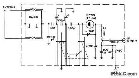
Uses self-oscillating funnel-diode converter circuit.- Transistor Manual, Seventh Edition, General Electric Co., 1964, p 359. (View)
View full Circuit Diagram | Comments | Reading(687)
Convenient And Simple High-Pass Filter (Differentiator) Circuit
Published:2011/7/30 19:37:00 Author:Robert | Keyword: Convenient, Simple, High-Pass, Filter, Differentiator
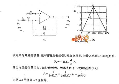
The picture shows the convenient and simple high-pass filter (differentiator) circuit.
This circuit is high-pass filter and also could be used as pulse differentiator. The relations between output voltage Ua and input voltage Ue is:Ua=-R1C1(d/dt)Uc.The output voltage's variation value is about 12dB/octave. The frequency point could be determined by the two formulas (picture b).fa=1/2πR1C1=1/2πR2C2, fb=1/2πR2C1.The resistor R3's value is equal with R2's value. (View)
View full Circuit Diagram | Comments | Reading(790)
Low_cost_instrumentation_amplifier
Published:2009/7/23 21:49:00 Author:Jessie
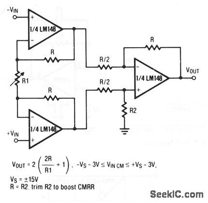
Compare this simple low-cost circuit to that of Fig 10-15. (View)
View full Circuit Diagram | Comments | Reading(628)
Photoconductive_cell_amplifier
Published:2009/7/23 21:56:00 Author:Jessie
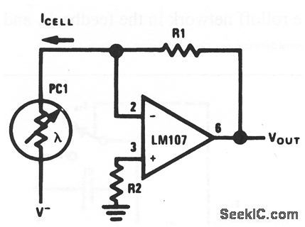
R1 depends on cell sensitivity, and should be chosen for eithermaxlmum dynamic range, Or for a desired scale factor. R2 is used tominimize outputoffset. and can be omitted in many applications. (View)
View full Circuit Diagram | Comments | Reading(843)
400_Hz_LED_OPAMP_SlNE_WAVE
Published:2009/7/5 22:47:00 Author:May
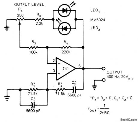
Uses LEDs as nonlinear- resistance diodes in Wien-bridge configuration with opamp operating from 15-V supply. Circuit will operate over wide range of other frequencies if values of R and C are changed. R5 adjusts output amplitude from 10 to 20 V P-P. Total harmonic distortion is 15%.-W. G. Jung, LED's Do Dual Duty in Sine-Wave Oscillator, EDN Magazine, Aug. 20, 1976, p 84-85. (View)
View full Circuit Diagram | Comments | Reading(882)
Integrator
Published:2009/7/23 21:54:00 Author:Jessie
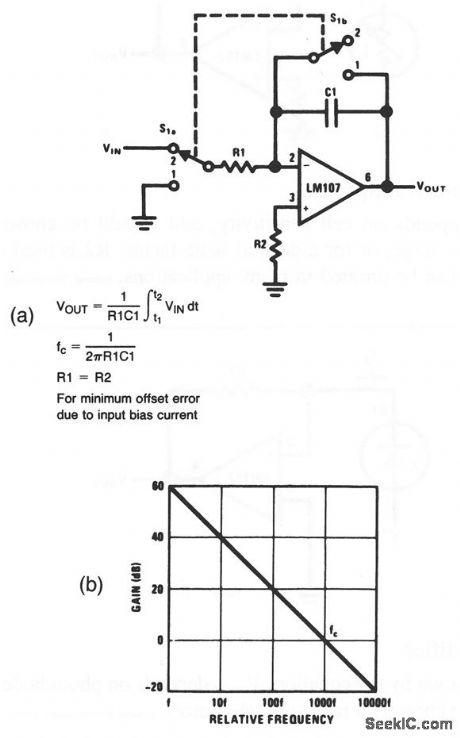
This circuit was originally developed to perform the mathematical operation of integration in analog computers. As shown by the frequency-response plot of Fig. 10-41B, an integrator is essentially a low-pass filter with a frequency response that decreases at 6 dB per octave. When S1 is in position 1, the amplifier is connected in unity gain, and C1 is discharged, which sets an initial condition of zero volts. With S1 in position 2, the amplifier is connected as an integrator, where the output changes in accordance with a constant times the time integral of the input. (View)
View full Circuit Diagram | Comments | Reading(1462)
HIGH_SPEED_PAPER_TAPE_READER
Published:2009/7/5 22:32:00 Author:May
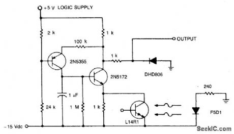
When computer peripheral equipment is interfaced, it is convenient to work with logic signal levels. With a nominal 4V at the output dropping to -0.6V on illumination, this circuit reflects the requirements of a high-speed, paper tape optical reader system.
The circuit operates at rates of up to 1000 bits per second. It will also operate at tape translucency such that 50% of the incident light is transmitted to the sensor, and provide a fixed threshold signal to the logic circuit, all at low cost. Several circuit tricks are required. Photodarlington speed is enhanced by cascode constant voltage biasing. The output threshold and tape translucency requirements are provided for by sensing the output voltage and operating to 2000 bits per second at ambient light levels equal to signal levels. (View)
View full Circuit Diagram | Comments | Reading(748)
Sampling Error Amplifier Intergrated Circuit of SE135N
Published:2011/7/29 0:30:00 Author:Michel | Keyword: Sampling Error, Amplifier, Intergrated Circuit
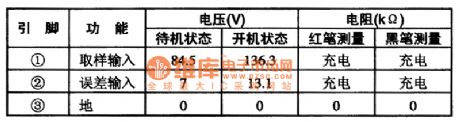
SE135N is a sampling error amplifier intergrated circuit and it is widely used in big screen color TV ,VCD,DVD and kinds of switch power supply.
First,Functions Features
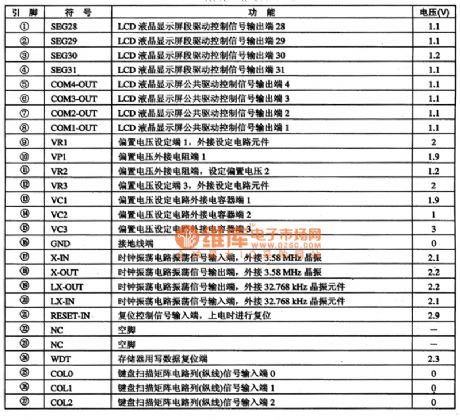
SE135N integrated circuit contains sampling voltage processing circuit, error signal processing circuit, and some other auxiliary function circuit. SE135N IC adopts feet 35 single encapsulation method and its pins functions and data is shown as table 1.
Table 1:SE135N IC Pins Functions and Data (View)
View full Circuit Diagram | Comments | Reading(775)
General_purpose_RF_amplifier
Published:2009/7/23 22:16:00 Author:Jessie
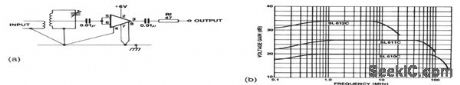
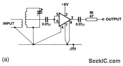
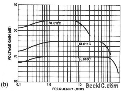
This circuit is suitable for an SL610C, SL611C, or SC612C. Figure 2-29B-shows the typical voltage gains for the three amplifiers. (View)
View full Circuit Diagram | Comments | Reading(723)
S1493 Communication Single-chip Microcomputer Integrated Circuit
Published:2011/7/29 8:53:00 Author:Michel | Keyword: Communication Single-chip, Microcomputer, Integrated Circuit
S1493 is a communication single-chip microcomputer integrated circuit, which is widely used in a multi-function call display telephone,such as the 2000 series phones.
First,Functions Features
S1493 integrated circuit is mainly used to complete pulse/double audio dial-up, FSK/DTIMF (frequency shift keying/a frequency system) calling display. Computer controls signal input and output.
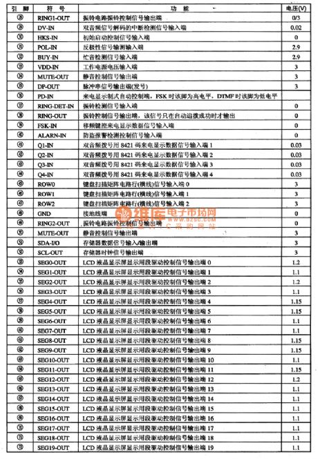
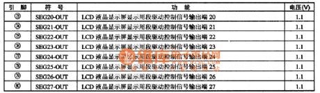
Second,Pins Functions and DataS1493 microcomputer integrated circuit uses 80 pins soft packaging way.The liquid crystal display chip packages is directly packaged on printed circuit boards.This structure can greatly improve the reliability of the circuit and also reduce the cost of the circuit.Its pins functions and data are shown as table 1.
Table 1:S1493 IC Pins and Data
(View)
View full Circuit Diagram | Comments | Reading(570)
Programmable_gain_amplifier
Published:2009/7/23 22:16:00 Author:Jessie
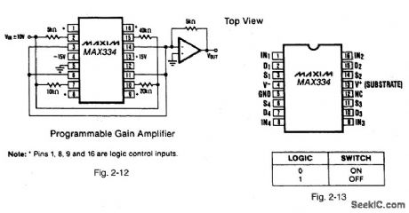
Figures 2-12 and 2-13 show a typical application circuit and pin configuration/ logic, respectively, for the MAX334, which is a direct replacement for the Siliconix DG271 and HI-201HS. The IC has guaranteed break-before-make switching, tON of 100 ns, tOFF of 50 ns, and channel-on resistance of 50 Ω(max). Split supplies (±5 V to ±15 V) or single positive supplies (+5 V to +30 V) can be used without affecting switching speed or the CMOS/TTL logic-compatible inputs. MAXIM HIGH-RELIABILITY DATA Book, 1993, P. 1-17. (View)
View full Circuit Diagram | Comments | Reading(0)
OPERATIONAL_AMPUFIER_SAMPLER
Published:2009/7/23 22:16:00 Author:Jessie
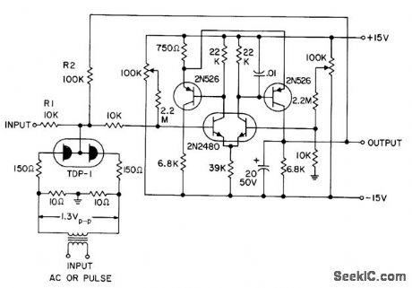
Uses funnel-diode pair with amplifier to provide output that is proportional to input signal at instant corresponding to leading edge of sampling pulse. Voltage gain of circuit is 100.Can also be used to measure differential peak point current of tunnel diode pairs.- Transistor Manual, Seventh Edition, General Electric Co., 1964, p 372. (View)
View full Circuit Diagram | Comments | Reading(736)
MB3759 Charging Circuit
Published:2011/7/23 0:16:00 Author:Michel | Keyword: Charging Circuit
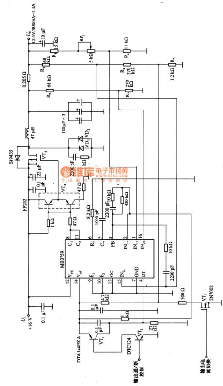
The above pictutre is MB3759 charging circuit.The adjustable output voltage of charging circuit is 12.6 V and output current is 1300 mA or 400 mA.It can charge eight series nimh batteries or 3 quarter series lithium batteries.Its output voltage is set by R1,R2 and RP1.R2 voltage value can be increased by improving output voltage.The output current is controlled by VT3 signal and regulated by R3~R7.And the controlled output current is 1300mA or 400mA.
(View)
View full Circuit Diagram | Comments | Reading(2584)
CLOSED_RING_COUNTER
Published:2009/7/23 22:04:00 Author:Jessie

Serves as 20-channel electronic switch for sampling voltage sources at rates of up to 50,000 cps. Flip-flop ring actuates diode gates in step with trigger pulses. Output can be used to drive recorders or feed data processing equipment.-K. L. Bents and B. E. Bishop, High-Speed Multiplexing With Closed-Ring Counters, Electronics, 32-26, p 48-50. (View)
View full Circuit Diagram | Comments | Reading(964)
AM_SSB_CW_IF_strip
Published:2009/7/23 22:03:00 Author:Jessie
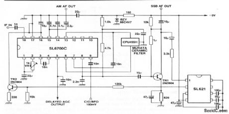
This circuit shows an SL6700C(Fig.2-13)connected to form an AM/SSB/CW IF strip.The SL621 is an AGC generator that is designed specifically for SSB operation. (View)
View full Circuit Diagram | Comments | Reading(1769)
CXAl261M (TV) infrared remote control receiving preamplifier circuit
Published:2011/8/1 8:20:00 Author:Christina | Keyword: TV, infrared, remote control, receiving, preamplifier circuit
The CXAl261M is designed as the silicon monolithic integrated circuit. It has the same technical characteristics, absolute maximum ratings, main electrical specifications, logic diagram and typical application circuits with the CX20106A excepts the shape structure.
(View)
View full Circuit Diagram | Comments | Reading(553)
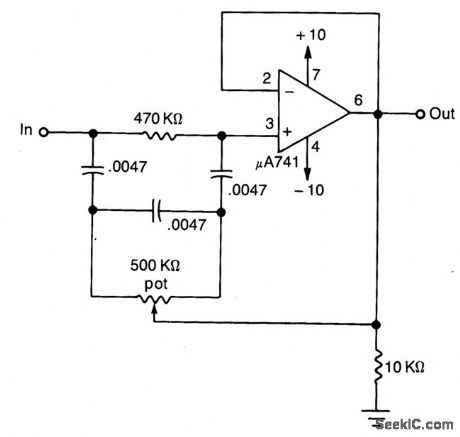
VARIABLE_GAIN_AND_SIGN_OP_AMP_CIRCUIT
Published:2009/7/5 22:15:00 Author:May
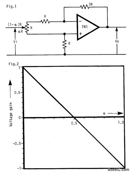
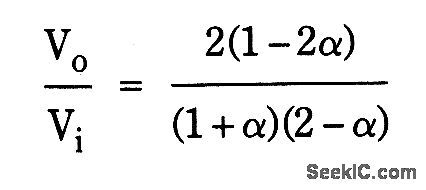
The gain of the amplifier is smoothly controllable between the limits of +1 to -1.It is adjustable over this range using a single potentiometer. The voltage gain of the arrangement is given by:
Where ct represents the fractional rotation of the potentiometer. (View)
View full Circuit Diagram | Comments | Reading(764)
TUNABLE_NOTCH_FILTER_USES_AN_OPERATIONAL_AMPLIFIER
Published:2009/7/5 22:11:00 Author:May
This notch filter is useful for tunable band-reject applications in the audio range. The values shown will give a tuning range of about 300-1500 Hz. (View)
View full Circuit Diagram | Comments | Reading(837)
BALANCE_AMPLIFIER_WITH_LOUDNESS_CONTROL
Published:2009/7/5 22:01:00 Author:May

View full Circuit Diagram | Comments | Reading(902)
| Pages:121/250 At 20121122123124125126127128129130131132133134135136137138139140Under 20 |
Circuit Categories
power supply circuit
Amplifier Circuit
Basic Circuit
LED and Light Circuit
Sensor Circuit
Signal Processing
Electrical Equipment Circuit
Control Circuit
Remote Control Circuit
A/D-D/A Converter Circuit
Audio Circuit
Measuring and Test Circuit
Communication Circuit
Computer-Related Circuit
555 Circuit
Automotive Circuit
Repairing Circuit