
Amplifier Circuit
Index 132
GATED_ASTABLE
Published:2009/7/2 0:24:00 Author:May
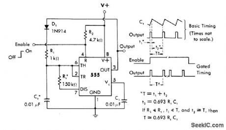
With values shown, circuit produces positive output pulses at about 1 kHz when gated on by positive pulse at pin 4. Supply voltage for 555 timer can be 15V.-W. G. Jung, IC Timer Cookbook, Howard W. Sams, Indianapolis, IN, 1977, p 135-136. (View)
View full Circuit Diagram | Comments | Reading(1120)
POSITIVE_INPUT_GIVES_GREEN
Published:2009/7/1 23:58:00 Author:May
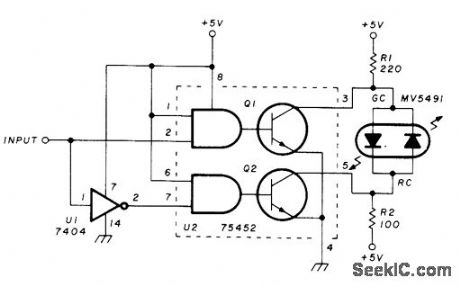
High or positive input to circuit gives green indication in Monsanto MV5491 dual red/green LED, and low input gives red. Circuit uses single SN75452 IC INPUT driver and one section of SN7404 hex nverter.-K. Powell, Novel Indicator Circuit,Ham Radio, April 1977, p 60-63. (View)
View full Circuit Diagram | Comments | Reading(796)
PIANO_TUNING_AMPLIFIER
Published:2009/7/1 23:58:00 Author:May
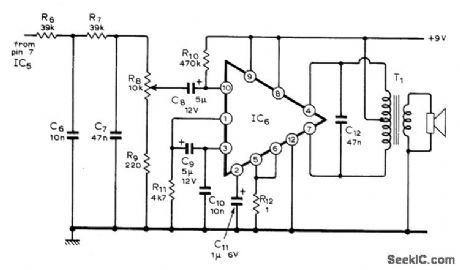
Used with battery-powered digital tuning aid that provides 12 equal semitones of octave, between 261.6625 and 493.8833 Hz, for equal-temperamenttuning of such keyboard instruments as organ. piano. and harpsichord. IC used is part of RCA amplifier kit KC-4003 which includes T1 and other discrete components. Article gives circuits for oscillator and programmable divider, along with instructions for construction. calibration. and use.-W.S. Pike. Digital Tuning Aid. Wireless World. July 1974. p 224-227. (View)
View full Circuit Diagram | Comments | Reading(794)
RF_SNIFFER
Published:2009/7/1 23:56:00 Author:May
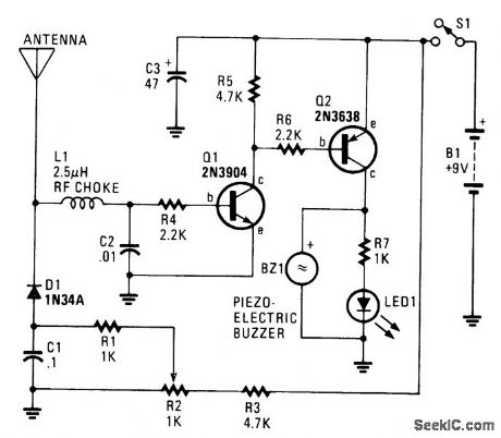
This circuit responds to RF signals from below the standard broadcast band to well over 500 MHz, and provides a visual and audible indication when a signal is received.The circuit is designed to receive low-powered signals as well as strong sources of energy by adjusting the bias on the pick-up diode, D1, with R2. A very sensitive setting can be obtained by carefully adjusting R2 until the LED just begins to light and a faint sound is produced by the Piezo sounder. (View)
View full Circuit Diagram | Comments | Reading(1629)
OPAMP_DRIVESLED
Published:2009/7/1 23:19:00 Author:May
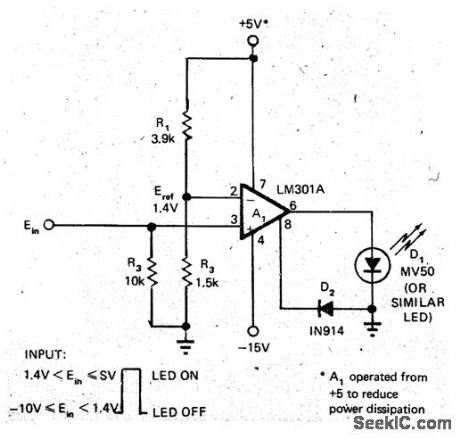
LM301A is used as open-Ioop voltage comparator, with LED receiving total source current of about 20 mA from opamp. Input is TTL-compatible, with R1-R2 reference divider biasing opamp in center of TTL output transition region. Circuit realizes full open-loop speed of opamp since it is uncompensated and its internal voltage amplifier stages are kept out of saturation by clamping of D2 and by inherent current-limiting action. Response times for toggling LED are in microsecond range.-W. G. Jung, Poor Man's LED Driver is TTL Compatible, EDN Magazine, Feb.5, 1973, p 86. (View)
View full Circuit Diagram | Comments | Reading(1320)
CAPACITANCE_MULTIPLIER
Published:2009/7/1 23:13:00 Author:May
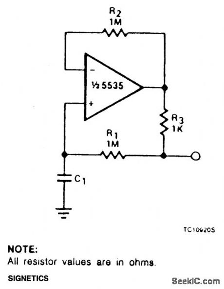
The circuit can be used to simulate large capacitances using small value components.With the values shown and C - 10 μF, an effective capacitance of 10,000 μF was obtained.The Q available is limited by the effective series resistance. So R1 should be as large as practical. (View)
View full Circuit Diagram | Comments | Reading(0)
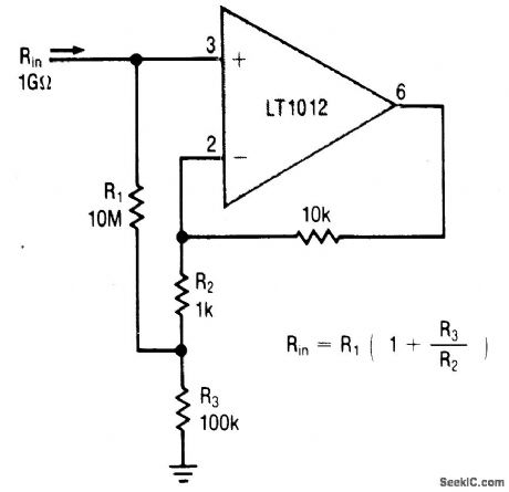
RESISTOR_MULTIPLIER
Published:2009/7/1 23:11:00 Author:May
View full Circuit Diagram | Comments | Reading(1460)
Single_cell_microphone_amplifier
Published:2009/7/24 3:06:00 Author:Jessie
As shown, the circuit provides a voltage-gain of 60 dB over a 5-kHz bandwidth, loaded at 500 Ω. Unloaded, it is possible to get 60-dB gain up to 10 kHz. Input impedance is 10 kΩ. Notice that with a single cell, the output cannot swing much below 150 mV, nor closer than 800 mV to the supply. Input noise is 40 to 50 nV/√Hz (about equal to the op amp). (View)
View full Circuit Diagram | Comments | Reading(671)
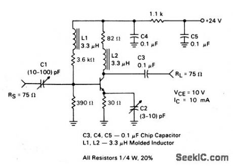
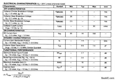
400_MHz_60_W_amplifier_28_V_supply
Published:2009/7/24 3:06:00 Author:Jessie
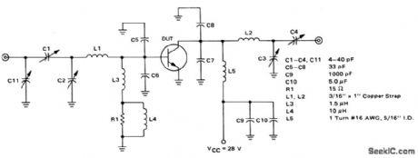
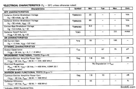
The electrical characteristics for the 2N6439 shown in this circuit are given in Fig.2-39B. (View)
View full Circuit Diagram | Comments | Reading(651)
VOLTAGE_CONTROLLED_AMPLIFIER
Published:2009/7/1 22:12:00 Author:May

Gain is linearly controlled by sum of input control voltages and a bias voltage, to provide amplitude modulation as required for synthesizer used to generate wide variety of sounds. Heart of circuit is linear four-quadrant multiplier IC. Output is taken between two load resistors, with differential amplifier IC2 removing common-mode signal Article describes operation In detail and glves all other circuits of synthesizer.along with procedure for aligning preset controls R8、R14.R20.and R21,-T Orr and D VV Thomas、ElectroniC Sound Synthesizer、Wireless World.、Part2-Sept .1973、p429-434(Part 1-Aug 1973.p366-372;Part 3-Oct 1973.p485-490) (View)
View full Circuit Diagram | Comments | Reading(0)
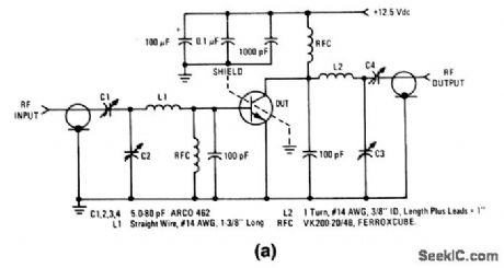
175_MHz_40_W_amplifier_125_V_supply
Published:2009/7/24 3:01:00 Author:Jessie
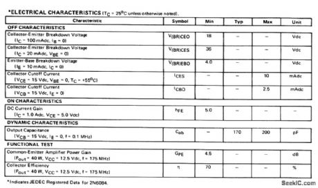
The electrical characteristics for the 2N6083 shown in this circuit are given in Fig.2-37B. (View)
View full Circuit Diagram | Comments | Reading(792)
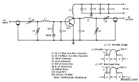
175_MHz_30_W_amplifier_125_V_supply
Published:2009/7/24 3:00:00 Author:Jessie
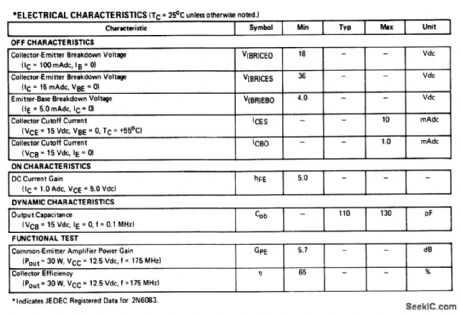
The electrical characteristics for the 2N6083 shown in this circuit are given in Fig.2-36B. (View)
View full Circuit Diagram | Comments | Reading(1935)
150_MHz_100_W_amplifier_28_V_supply
Published:2009/7/24 3:03:00 Author:Jessie
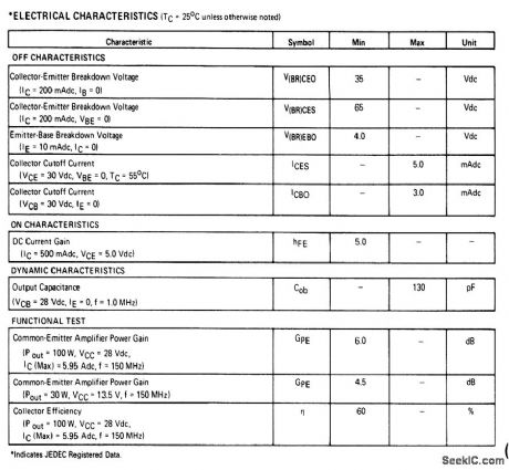
The electrical characteristics for the 2N6166 shown in this circuit are givenin Fig. 2-38B. (View)
View full Circuit Diagram | Comments | Reading(1048)
LOW_DISTORTION_LOW_LEVEL_AMPLITUDE_MODULATOR
Published:2009/7/1 21:27:00 Author:May
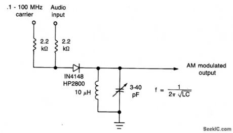
This simple diode modulator delivers excellent results when used for high percentage modulation at low signal levels. Constants are shown for a carrier frequency of about 10 MHz, but, with a suitable tank, the circuit will give good results at any frequency at which the diode approximates a good switch. To extend frequency above that for which the IN4148 is suited, a hot-carrier diode (HP2800, etc.) can be substituted. A shunt resistor across the tank circuit can be used to reduce the circuit Q so as to permit high percentage modulation without appreciable distortion. (View)
View full Circuit Diagram | Comments | Reading(3543)
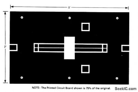
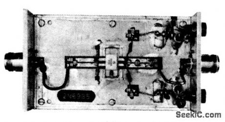
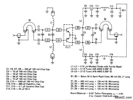
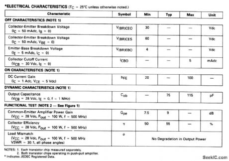
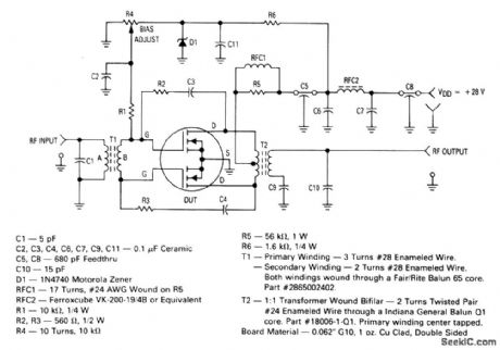
500_MHz_100_W_push_pull_amplifier
Published:2009/7/24 3:22:00 Author:Jessie
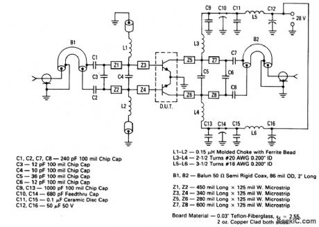
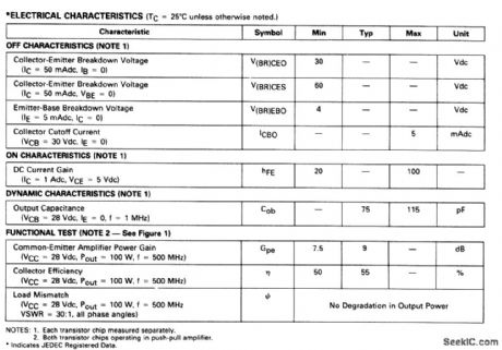
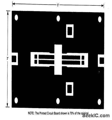
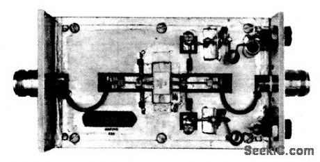
The electrical characteristics for the 2N6986(push-pull transistor)shown in this circuit are gilven in Fig.2-42B Figures 2-42C and 2-42D show the photomaster, and parts location, respectively. Those not familiar with microstrip techniques(for Z1 through Z8)should read the many Motorola publications, such as AN548A and AN555.
(View)
View full Circuit Diagram | Comments | Reading(813)
30_to_900_MHz_broadband_amplifier10_-V_supply
Published:2009/7/24 3:24:00 Author:Jessie
The electrical characteristics for the BFW92A shown in this circuit are given in Fig,2-43B. (View)
View full Circuit Diagram | Comments | Reading(874)
400_MHz_125_W_push_pull_amplifier
Published:2009/7/24 3:18:00 Author:Jessie
The electrical characteristics for the 2N6985 (push-pull transistor ) shown in this circuit are given in Fig .2-41B. Figures 2-41C and 2-41D show the photomaster ,and parts location , respctively, Those not familiar with microstrip techniques (for Z1 through Z5) should read the many Motorola publications, such as AN548A and AN555. (View)
View full Circuit Diagram | Comments | Reading(886)
TREMOLO_AMPLlFIER
Published:2009/7/1 20:40:00 Author:May
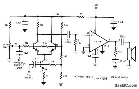
Provides amplitude modulation at subaudio rate (usually between 5 and 15 Hz) of audio-frequency input signal. Uses National LM389 attay having three transistors along with power amptifier. Transistors form differential pair having active currentsource tail to give output proportional to product of two input signals. Gain control pot is adjusted for desired tremolo depth. Interstage RC network forms 1 60-Hz high-pass filter, requMng that tremolo frequency be tess than 160 Hz.- Audio Handbook, National Semiconductor, Santa Clara, CA, 1977, p 4-33-4-37. (View)
View full Circuit Diagram | Comments | Reading(751)
WINDICATOR
Published:2009/7/1 20:37:00 Author:May

Circuit Notes
Two TTL ICs and a handful of other com-ponents are all that is needed for a circuit that will indicate which of four buttons was pressed first, as well as lock out all other entries. A logic 0 at one of the Q outputs, lights the ap; propriate LED and locks out other entries by taking the clock input low. (View)
View full Circuit Diagram | Comments | Reading(672)
30_to_150_MHz_30_W_MOS_amplifier_28_V_supply
Published:2009/7/24 3:37:00 Author:Jessie
The electrical characteristics for the MRF136Y shown in this circuit are given in Fig. 2-2-48B. (View)
View full Circuit Diagram | Comments | Reading(543)
| Pages:132/250 At 20121122123124125126127128129130131132133134135136137138139140Under 20 |
Circuit Categories
power supply circuit
Amplifier Circuit
Basic Circuit
LED and Light Circuit
Sensor Circuit
Signal Processing
Electrical Equipment Circuit
Control Circuit
Remote Control Circuit
A/D-D/A Converter Circuit
Audio Circuit
Measuring and Test Circuit
Communication Circuit
Computer-Related Circuit
555 Circuit
Automotive Circuit
Repairing Circuit