
Amplifier Circuit
Index 126
Chopper_stabilized_instrumentation_arnplifier
Published:2009/7/23 23:17:00 Author:Jessie

This circuit is similar to that of Fig. 1-4, but uses the remaining LTC1043 (Fig. 1-4B) section to form a low-drift chopper amplifier. The approach maintains the true differential inputs, while achieving 0.1-μV/℃ drift. (View)
View full Circuit Diagram | Comments | Reading(922)
IC_amplifier_with_high_current_booster
Published:2009/7/23 23:22:00 Author:Jessie
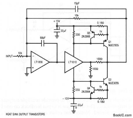
This circuit is capable of delivering a 3-A output current (±10 V) with a bandwidth of 100kHz, and a slew-rate of about 10 V/μs. (View)
View full Circuit Diagram | Comments | Reading(1129)
Simple_video_line_splitter_
Published:2009/7/23 23:20:00 Author:Jessie
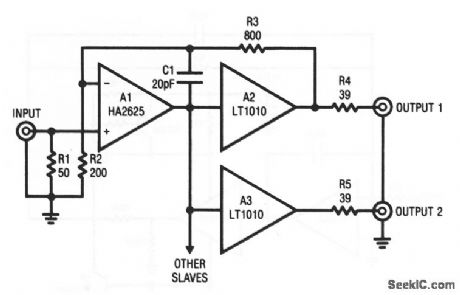
This circuit shows a simple way to provide multiple outputs for a single input (at video frequencies). The technique is to put feedback on one buffer, with the remaining buffers slaved. Notice that offset and gain accuracy of the slave buffers depends on the matching with the master. (View)
View full Circuit Diagram | Comments | Reading(2910)
PREFERRED_HIGHLEVEL_AMPLIFIER
Published:2009/7/23 23:20:00 Author:Jessie
Linear pulse voltage amplifier, designed primarily as crt intensity modulation device, has minimum bandwidth of 3 Mc. Takes positive input pulses and gives maximum negative output of 55 v.-NBS, Handbook Preferred Circuits Navy Aeronautical Electronic Equipment, Vol. II, Semiconductor Device Circuits, PSC 20 (originally PC 220), p 20-2. (View)
View full Circuit Diagram | Comments | Reading(734)
DARLINGTON_PAIR_SERVO_AMPLIFIER
Published:2009/7/23 23:19:00 Author:Jessie
Open-loop gain of differential forward amplifier Q1 through Q8 is over 2,000 and dosed-loop gain is 200. Signal across output of common-mode feedback amplifier Q9-Q10 is differentially summed by R21-R22 to cancel a-c components, while d-c component is amplified and applied to emitters of differential-input Darlington pair.-M. W. Aarons, Putting a Servo Amplifier on a Small Silicon Wafer, Electronics, 35:52, p 33-35. (View)
View full Circuit Diagram | Comments | Reading(692)
140_W_PEP_2__to_30_MHz_amateur_radio_linear_amplifier
Published:2009/7/23 23:19:00 Author:Jessie
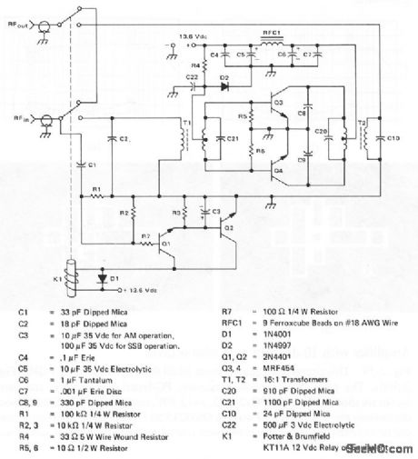
Both the parts and kits for this amplifier are available from: Commu-nications Concepts, 121 Brown St. Dayton, Ohio 45402, (513) 220-9677. Use of this amplifier is illegal for the class-D citizen band. (View)
View full Circuit Diagram | Comments | Reading(623)
Common_emitter_output_stage_with_voltage_gain
Published:2009/7/23 23:26:00 Author:Jessie
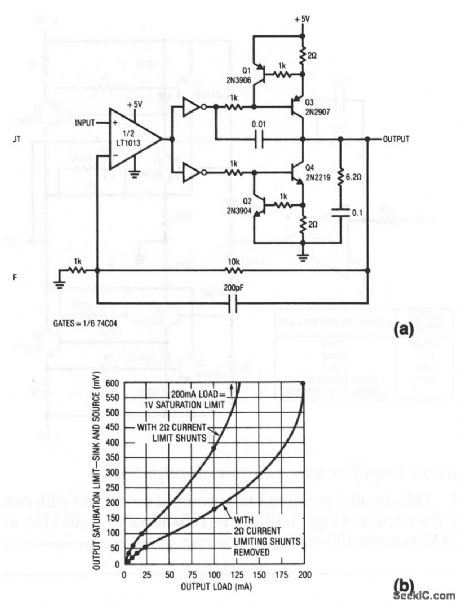
This circuit is similar to that of Fig. 1-10, except that the CMOS inverters drive bipolar transistors to reduce saturation losses, even at relatively high currents. Fig. 1-11B shows the output saturation characteristics. (View)
View full Circuit Diagram | Comments | Reading(814)
200_MHz_cascode_amplifier
Published:2009/7/23 23:29:00 Author:Jessie
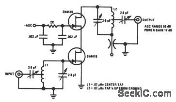
This JFET cascode circuit features low crossmodulation, large-signal handling ability, no neutralization, and an AGC that is controlled by biasing the upper cascode JFET. The only special requirement of this circuit is that IDSS of the upper JFET must be greater than that of the lower JFET. (View)
View full Circuit Diagram | Comments | Reading(0)
Amplifier_with_±120_V_output_
Published:2009/7/23 23:29:00 Author:Jessie
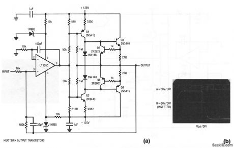
This amplifier provides a±120-V output. The full-power bandwidth is 15-kHz with a slew rate of about 20 V/μs. Figure 1-13B shows the results with a ±12-V input (trace A). The output (trace B) is a cleanly-damped 240 Vpp pulse. (View)
View full Circuit Diagram | Comments | Reading(776)
High_current_amplifier_with_rail_to_rail_output
Published:2009/7/23 23:27:00 Author:Jessie

This circuit features rail-to-rail output swing, but with currents higher than with the circuits of Figs. 1-10 and 1-11. Bandwidth is 600 kHz, and slew rate exceeds 24 V/μs under 100-mA output loading. (View)
View full Circuit Diagram | Comments | Reading(1021)
Low_noise_dc_stabilized_amplifier
Published:2009/7/23 23:52:00 Author:Jessie
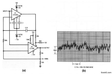


This circuit combines a low-drift chopper-stabilized amplifier with an ultra-low noise bipolar amplifier. The LTC1052 measures the dc error at the LT1028 input terminals, and biases the offset pins to force offset to a few microvolts. As a result, noise is kept to a minimum. The combined characteristics of these amplifiers yield the following: offset voltage = 5μV max. offset drift = 50 nV/℃, and noise 1.1 nV HZ. Figure 1-23B plots noise amplitude over time in a 0.1- to 10-Hz bandwidth. . (View)
View full Circuit Diagram | Comments | Reading(984)
DYNAMIC,CONSTANT_CURRENT_LOAD_FOR_FUEL_CELL_BATTERY_TESTING
Published:2009/7/3 4:20:00 Author:May
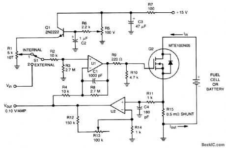
This circuit was designed for testing fuel cells, but it could also be used for testing batteries under a constant current load. It provides a dynamic, constant current load, eliminating the need to manually adjust the load to maintain a constant load.
For fuel cell application, the load must be able to absorb 20-40 A, and since a single cell develops only 0.5 to 1.0 V, bipolar power devices (such as a Darlington) are impractical. Therefore, this dynamic load was designed with a TMOS Power FET (Q2).
With switch S1 in position 1, emitter follower Q1 and R1 establish the current level for the load. In position 2, an extemal voltage can be applied to control the current level.
Operational amplifier U1 drives TM0S device Q1, which sets the load current seen by the fuel cell or battery. The voltage drop across R15, which is related to the load current, is then applied to U2, whose output is fed back to U1. Thus, if the voltage across R15 would tend to change, feedback to the minus input of U1 causes that voltage (and the load current) to remain constant. Adjustment of R13 controls the volts/amp of feedback. The VOUT point is used to monitor the system. (View)
View full Circuit Diagram | Comments | Reading(3190)
RAPID_BATTERY_CHARGER_FOR_ICOM_IC_2A
Published:2009/7/3 3:55:00 Author:May

Rectifted and filtered voltage from the 24 Vac transformer is applied to the LM723 voltage regulator and the npn pass transistor set up for constant current supply. The 470 ohm resistor limits trickle current until the momentary pushbutton (S2) is depressed, the SCR turns on and current ftows through the previously determined resistor network limiting the charging current. The SCR will turn off when the thennal cutout circuit inside the battery pack opens up. (View)
View full Circuit Diagram | Comments | Reading(3022)
ACTIVE_CLAMP_LIMITING_AMPLIFIER
Published:2009/7/3 3:52:00 Author:May
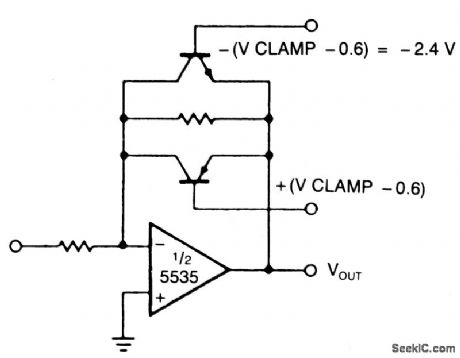
The modified inverting amplifier uses an active clamp to limit the output swing with precision.Allowance must be made for the VBEof the transistors. The swing is limited by the base- emitter breakdown of the transistors. A simple circuit uses two back-to-back zener diodes across the feedback resistor, but tends to give less precise limiting and cannot be easily controlled. (View)
View full Circuit Diagram | Comments | Reading(1030)
DIFFERENTIAL_AMPLIFIER
Published:2009/7/3 3:50:00 Author:May
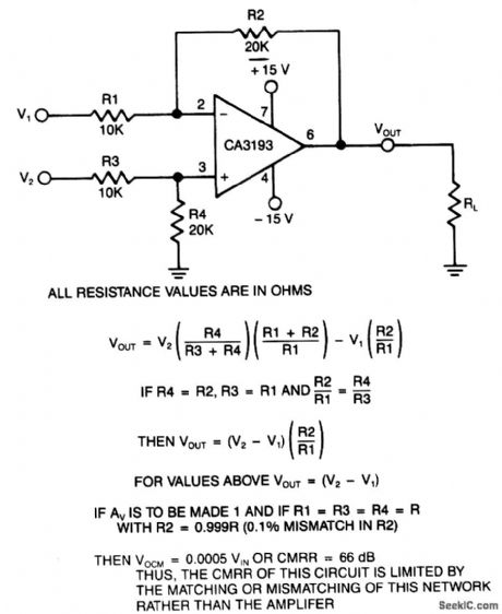
This differential amplifier uses a CA3193 BiMOS op amp. This classical, differential input-to-signal-ended output converter when used with lowresistance signal source will maintain level of CMRR, if R1=R3 + R4. (View)
View full Circuit Diagram | Comments | Reading(5095)
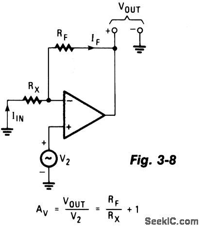
NONINVERTING_AMPLIFIER
Published:2009/7/3 3:48:00 Author:May

View full Circuit Diagram | Comments | Reading(0)
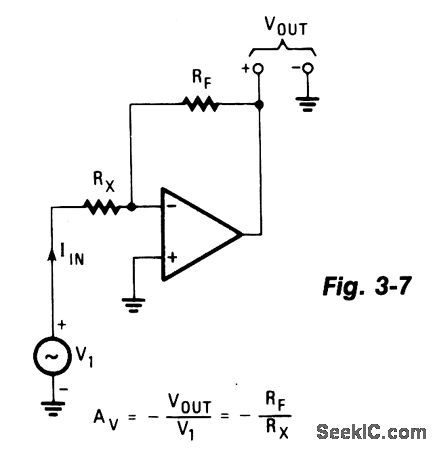
INVERTING_AMPLIFIER
Published:2009/7/3 3:47:00 Author:May
View full Circuit Diagram | Comments | Reading(0)
CASCADED_AMPLIFIER
Published:2009/7/3 3:46:00 Author:May
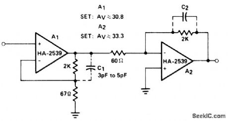
Cascaded amplifter sections are used to extend bandwidth and increase gain. Using two HA-2539 devices, this circuit is capable of 60-dB gain at 20 MHz. (View)
View full Circuit Diagram | Comments | Reading(1007)
SERVO_MOTOR_DRIVE_AMPLIFIER
Published:2009/7/3 3:45:00 Author:May

Digital ICs and opto-isolators provide the drive for this TMOS servo amplifier, resulting in fewer analog circuits and less drift. Fast and consistent turn-on and turn-off characteristics also enable accurate analog output results directly from the digital signal without the need for analog feedback.An H bridge configuration is employed for the servo amplifier, which obtains complementary PWM inputs from digital control circuits. The PWM inputs are applied via opto-isolators, which keep the digital control logic isolated from the 75 V supply used for the amplifier. A short circuit indicator is provided by opto-isolator U3; if there is a short, the drop across R9 increases to a value sufficient to activate the isolator and send a short indication to the digital control logic. (View)
View full Circuit Diagram | Comments | Reading(3763)
COMPOSITE_AMPLIFIER
Published:2009/7/3 3:45:00 Author:May


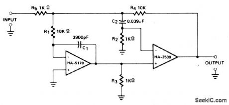

A composite configuration greatly reduces dc errors without compromising the high-speed, wideband characteristics of HA-2539. The HA-2540 could also be used, but with slightly lower speeds and band-width response.The HA-2539 amplifies signals above 40 kHz which are fed forward via C2; R2 and R5 set the voltage gain at -10. The slew rate of this circuit was measured at 350 V/μs. Settiing time to a 0.1% level for a 10-V output step is under 150 ns and the gain bandwidth product is 300 MHz.The HA-5170 ampliftes signals below 40 kHz, as set by C1 and R1, and controls the dc input charac-teristics such as offset voltage, drift, and bias currents of the composite amplifter. Therefore, it has an offset voltage of 100 μV, drift of 2 μV/'℃, and bias currents in the 20-pA range. The offset voltage can be externally nulled by connecting a 20-KΩ pot to pins 1 and 5, with the wiper tied to the negative supply.The dc gains of the HA-5170 and HA-2539 are cascaded; this means that the dc gain of the composite amplifier is well over 160 dB.The excellent ac and dc performance of this composite amplifter is complemented by its low noise performance, 0.5-μV rms from 0.1 Hz to 100 Hz. It is very useful in high-speed data acquisition systems. (View)
View full Circuit Diagram | Comments | Reading(0)
| Pages:126/250 At 20121122123124125126127128129130131132133134135136137138139140Under 20 |
Circuit Categories
power supply circuit
Amplifier Circuit
Basic Circuit
LED and Light Circuit
Sensor Circuit
Signal Processing
Electrical Equipment Circuit
Control Circuit
Remote Control Circuit
A/D-D/A Converter Circuit
Audio Circuit
Measuring and Test Circuit
Communication Circuit
Computer-Related Circuit
555 Circuit
Automotive Circuit
Repairing Circuit