
Amplifier Circuit
Index 134
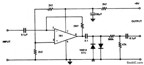
GUITAR_FUZZ
Published:2009/7/1 4:04:00 Author:May
Circuit Notes
The 741 has a maximum gain of 20,000,but the circuit is so designed that the IC’s gain is 2,700,000 which then distorts the output. This distortion gnres the fuzz effect. The two diodes clip the output to drop the level, also lowered by the potential divider. This circuit also sustains the notes, due to clipping, giving a totally new sound. (View)
View full Circuit Diagram | Comments | Reading(990)
COMPOSITE_AMPLIFIER
Published:2009/7/1 4:03:00 Author:May
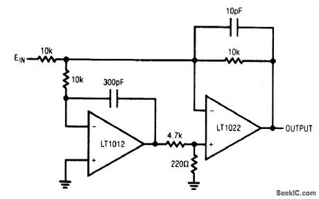
The circuit is made up of an LT1012 low drift device, and an LT1022 high speed amplifter. The overall circuit is a unity gain inverter, with the summing node located at the junction of three 10 k resistors. The LT1012 monitors this summing node, compares it to ground, and drives the LT1022's positive input, completing a dc stabilizing loop around the LT1022. The 10 k - 300 pF time constant at the LT1012 limits its response to low frequency signals. The LT1022 handles high frequency inputs while the LT1012 stabilizes the dc operating point. The 4.7 k - 220 ohm divider at the LT1022 prevents excessive input overdrive during start-up. This circuit combines the LT1012's 35 μV offset and 1.5 V/℃ drift with the LT1022's 23 V/μs slew rate and 300 kHz full power bandwidth. Bias current, dominated by the LT1012, is about 100 pA. (View)
View full Circuit Diagram | Comments | Reading(1512)
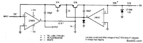
LOGARITHMIC_AMPLIFIER_2
Published:2009/7/1 4:01:00 Author:May
View full Circuit Diagram | Comments | Reading(600)
ULTRA_HIGH_ZSUBin_SUBAC_UNITY_GAIN_AMPLIFIER_
Published:2009/7/1 4:00:00 Author:May
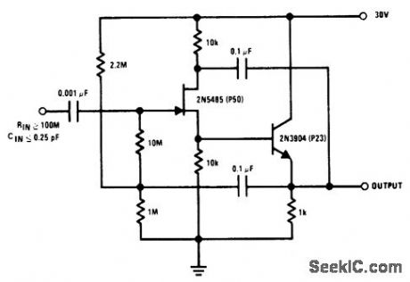
Nothing is left to chance in reducing inputcapacitance.The 2N5485,which has low capacitance in the first place,is operated db a sourcefollower with bootstrapped gate bias resistorand drain. (View)
View full Circuit Diagram | Comments | Reading(803)
ULTRA_LOW_LEAKAGE_PREAMPLIFIER_
Published:2009/7/1 3:59:00 Author:May
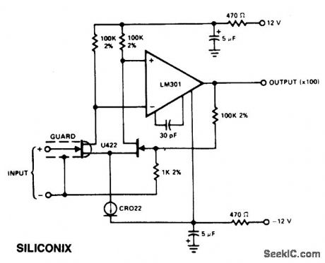
The circuit has an input leakage of only 2 pA typical at 75℃ and would be usable with1 M ohm input resistance. (View)
View full Circuit Diagram | Comments | Reading(670)
FET_INPUT_AMPLIFIER
Published:2009/7/1 3:58:00 Author:May
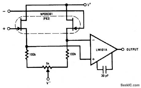
The NPD8301 monolithic-dual provides anideal low offset,low drift buffer function for the LM101A op amp, The excellent matchingcharacteristics of the NPD8301 track well overits bias current range,thus improving common-mode rejection. (View)
View full Circuit Diagram | Comments | Reading(748)
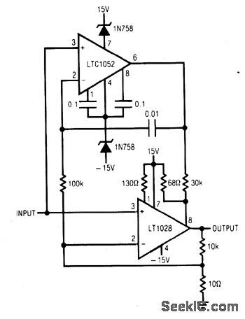
CHOPPER_STABILIZED_AMPLIFIER_
Published:2009/7/1 3:58:00 Author:May
View full Circuit Diagram | Comments | Reading(693)
STABLE_UNITY_GAIN_BUFFER_WITH_GOOD_SPEED_AND_HIGHINPUT_IMPEDANCE
Published:2009/7/1 3:47:00 Author:May
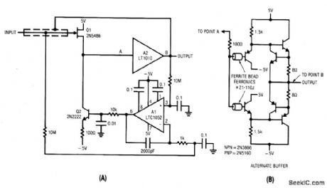
Q1 and Q2 constitute a simple, high speed FET input buffer. Q1 functions as a source follower, with the Q2 current source load setting the drain-source channel current.Normally, this open loop configuration would be quite drifty because there is no dc feedback. The LTC1052 contributes this function to stabilize the circuit by comparing the filtered circuit ot,ttput to a similarly filtered version of the input signal. The amplified difference between these signals is used to set Q2's bias and hence Q1's channel current.This forces Q1's VGS to whatever voltage is required to match the circuit's input and output potentials. The 2000 pF capacitor at A1 provides stable loop compensation. The RC network in Al's output prevents it from seeing high speed edges coupled through Q2's collector-base junction. AZ's output is also fed back to the shield around Q1's gate lead, bootstrapping the circuit's effective input capacitance down to less than 1 pF. For very fast requirements, the alternate discrete component buffer shown will be useful.Although its output is current limited at 75 mA, the GHz range transistors employed provide exceptionally wide bandwidth, fast slewing and very little delay. (View)
View full Circuit Diagram | Comments | Reading(864)
MONOSTABLE_USING_VIDEO_AMPLIFIER_AND_COMPARATOR
Published:2009/7/1 2:47:00 Author:May
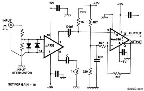
The output of a video amplifier is differentiated before being fed to a Schottky comparator. The propagation delay is reduced to typically 10ns. The output pulse width is set by the value of C, 100pf giving a pulse of about 90ns duration. (View)
View full Circuit Diagram | Comments | Reading(875)
PRECISION_REFERENCE_LOW_NOISSE_BUFFERED_REFERENCE
Published:2009/7/1 2:37:00 Author:May
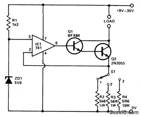
The circuit will provide 3 preset currents which will remain constant despite variations of ambient temperature or line voltage. ZD1 prifuces a temperature stable reference voltage which is applied to the noninverting input of IC1. 100% feedback is applied from the output to the inverting input holding the voltage at Q2s emitter at the same potential as the noninverting input. The current flowing into the load therefore is defined solely by the resistor selected by S1. Whic the values employed here, apreset current of 10 mA, 100 mA or 1 A van be selected. Q2 should be mounted on a suitabel heatsink. (View)
View full Circuit Diagram | Comments | Reading(707)
225_to_400_MHz_10_W_amplifier_28_V_supply
Published:2009/7/24 4:29:00 Author:Jessie
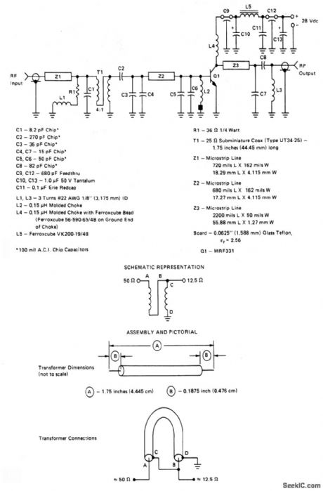
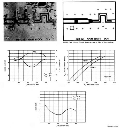
This amplifier can be used as is, or as a driver for higher-power devices. Figure 2-58B shows the construction details for transformer T1. Figures 2-58C and 2-58D show the component layout, and PC-board layout, respectively.Figures 2-58E, 2-58F, and 2-58G show typical amplifier performance characteristics. Those not familiar with microstrip techniques (for Z1, Z2, and Z3) should read the many Motorola publications, such as AN548A and AN555. (View)
View full Circuit Diagram | Comments | Reading(677)
2_to_30_MHz_300_W_PEP_linear_amplifier_28_V_suplly
Published:2009/7/24 4:27:00 Author:Jessie

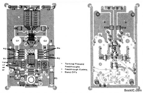
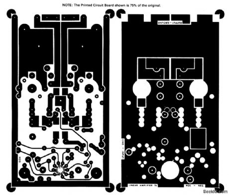
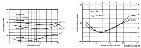
This push-pull linear amplifier provides 300-W of PEP Or CW output power across the 2-to 30-MHz band. The component layout, and PC-board layout, ale shown in Figs.2-57B and 2-57C, respectively,Both the parts and kits for this amplifier are available from: Communications Concepts, 121 Brown St., Dayton, Ohio 45402, (513) 220-9677. Use of this amplifier is illegal for class-D citizen band. (View)
View full Circuit Diagram | Comments | Reading(2286)
FM_tuner_with_single_tuned_detector_coil
Published:2009/7/24 4:33:00 Author:Jessie
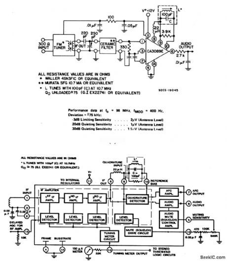
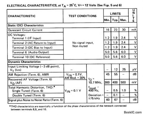
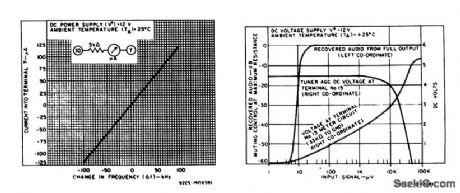
The CA3089 shown in this circuit includes an IF amplifier, quadrature detector, AF preamplifier, and specific circuits for AGC, AFC, muting (squelch), and tuning meter, as shown in Fig. 2-60B. Limiting sensitivity is 12μV (typical) at -3-dB point. The recovered audio is a typical 400 mV. Distortion (with a double-tuned coil) is a typical 0.1%. Typical characteristics are shown in Fig.2-60C. (View)
View full Circuit Diagram | Comments | Reading(1060)
225_to_400_MHz_60_W_amplifier_28_V_supply
Published:2009/7/24 4:31:00 Author:Jessie
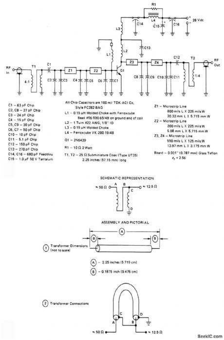
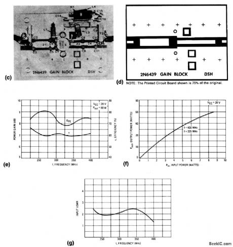
This amplifier can be used as is or two amplifiers can be combined with quadrature-couplers to form a 100-W amplifier. Figure 2-59B shows the construction details for transformers T1/T2, Figures 2-59C and 2-59D show the component layout, and PC-board layout, respectively. Figures 2-59E, 2-59F, and 2-59G show typical amplifier performance characteristics. Those not familiar with microstrip techniques (for Z1 through Z5) should read the many Motorola publications,such as AN548A and AN555. (View)
View full Circuit Diagram | Comments | Reading(771)
Linearized_platinum_RTD_resistance_bridge_switched_capacitor
Published:2009/7/24 5:15:00 Author:Jessie
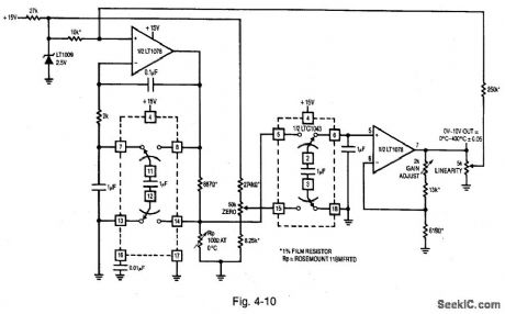
Figure 4-10 is a switched-capacitor version of the Fig. 4-9 circuit, with A2 and A3 replaced with an LTC1043. The differential-to-single-ended transitions in the current-source and bridge-output amplifier are performed by the LTC1043. The values shifts in the current source and output stage reflect the LTC1043 lack of gain. The primary trade-off between the two circuits is component count versus cost. LINEAR TECHNOLOGY, APPLICATION NOTE 43, P. 12. (View)
View full Circuit Diagram | Comments | Reading(992)
Low_noise_chopper_stabilized_bridge_amplifier
Published:2009/7/24 5:07:00 Author:Jessie
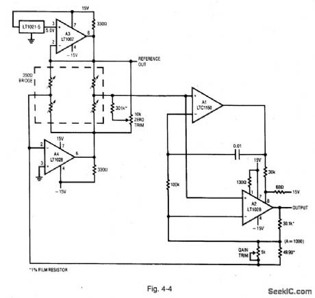
Figure 4-4 shows a circuit that is similar to that of Fig. 4-3, except that A1 is chopper stabilized. This reduces the offset error even further. A1 measures the dc error at the A2 inputs and biases the A1 offset pins to force an offset of a few microvolts. The offset-pin bias at A2 is arranged so that A1 will always be able to find the servo point.The 0.01-μF capacitor rolls off A1 at low frequencies, with A2 handling the high-frequency signals. Returning the A2 feedback string to the bridge midpoint eliminates the A4 offset contribution. If this was not done, A4 would require a similar offset-correction loop. The circuit has a drift of less than 0.05-μV/℃, 1-nV/Hz noise, and CMRR exceeding 160 dB. LINEAR TECHNOLOGY, APPLICATION Nom 43, P. 6. (View)
View full Circuit Diagram | Comments | Reading(772)
Low_noise_bridge_amplifier_with_common_mode_suppression
Published:2009/7/24 5:06:00 Author:Jessie
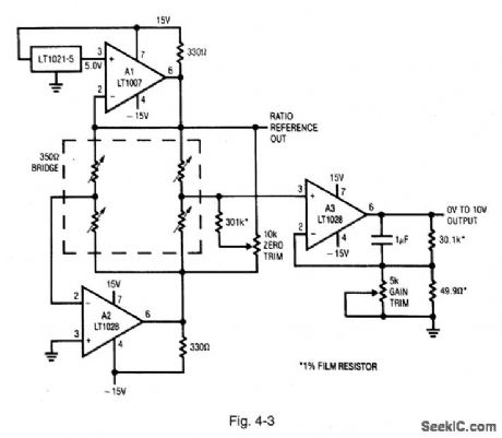
Figure 4-3 shows a circuit that is similar to that of Fig. 4-2, except that low-noise bipolar amplifiers are used. This circuit trades slightly higher dc offset drift for lower noise; it is a good candidate for stable resolution of small, slowly varying measurements. LINEAR TECHNOLOGY, APPLICATION NOTE 43, P. 6. (View)
View full Circuit Diagram | Comments | Reading(903)
Servo_controlling_bridge_drive
Published:2009/7/24 5:05:00 Author:Jessie
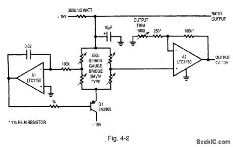
Figure 4-2 shows a way to reduce errors because of the bridge common-mode output voltage. A1 biases Q1 to servo the bridge left midpoint to zero under all operating conditions. The 350-Ω resistor ensures that A1 will find a stable operating point with 10 V of drive delivered to the bridge. This allows A2 to take a single-ended measurement, eliminating all common-mode voltage errors. LINEAR TECHNOLOGY, APPLICATION NOTE 43, P. 5. (View)
View full Circuit Diagram | Comments | Reading(862)
Bridge_based_instrumentation_amplifier
Published:2009/7/24 5:04:00 Author:Jessie
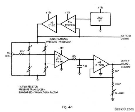
Figure 4-1 shows signal conditioning for a 350-Ω transducer bridge. The specified strain-gauge pressure transducer produces 3-mV output per volt of bridge excitation. The LT1021 reference, buffered by A1A and A2, drives the bridge. This potential also supplies the ratio output, permitting radiometric operation of a monitoring analog-to-digital converter (Chapter 8). Amplifier A3 extracts the bridge differential output at a gain of 100, with additional trimmed gain supplied by A1B. The circuit shown can be adjusted for a precise 10-V output at full-scale pressure. To trim the circuit, apply zero pressure to the transducer, adjust the 10-kΩ pot until the output just comes off 0 V. Then apply full-scale pressure and trim the 1-kΩ adjustment. Repeat the procedure until both points are fixed. LINEAR TECHNOLOGY, APPLICATION NOTE 43, P. 5. (View)
View full Circuit Diagram | Comments | Reading(1206)
OSCILLATOR_OR_AMPLIFIER_WITH_WIDE_FREQUENCY_RANGE
Published:2009/7/1 2:09:00 Author:May
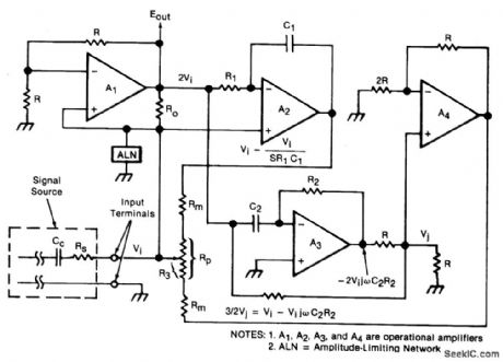
An oscillator/amplifter is resistively tunable over a wide frequency range. Feedback circuits containing operational amplifiers, resistors, and capacitors synthesize the electrical effects of an inductance and capacitance in parallel between the input terminals. The synthetic inductance and capacitance, and, therefore, the resonant frequency of the input admittance, are adjusted by changing a potentiometer setting. The input signal is introduced in parallel to the noninverting input terminals of operational amplifiers A1 and A2 and to the potentiometer cursor. The voltages produced by the feedback circuits in response to input voltage V1 are indicated at the various circuit nodes. (View)
View full Circuit Diagram | Comments | Reading(748)
| Pages:134/250 At 20121122123124125126127128129130131132133134135136137138139140Under 20 |
Circuit Categories
power supply circuit
Amplifier Circuit
Basic Circuit
LED and Light Circuit
Sensor Circuit
Signal Processing
Electrical Equipment Circuit
Control Circuit
Remote Control Circuit
A/D-D/A Converter Circuit
Audio Circuit
Measuring and Test Circuit
Communication Circuit
Computer-Related Circuit
555 Circuit
Automotive Circuit
Repairing Circuit