
Amplifier Circuit
Index 129
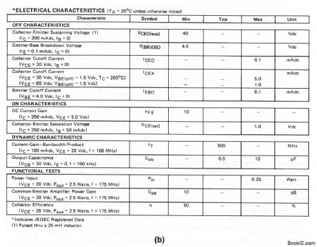
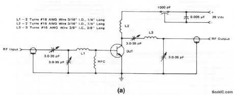
450_MHz_high_gain_amplifier_10_V_supply
Published:2009/7/24 2:27:00 Author:Jessie
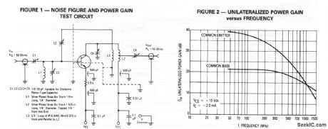
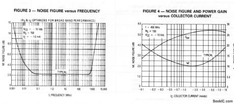
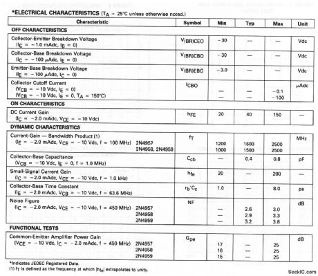
The electrical characteristics for the 2N4957,2N4958,and 2N4959 shown in this circuit are given in Fig.2-18B. (View)
View full Circuit Diagram | Comments | Reading(959)
600_Hz_NOTCH
Published:2009/7/2 21:10:00 Author:May
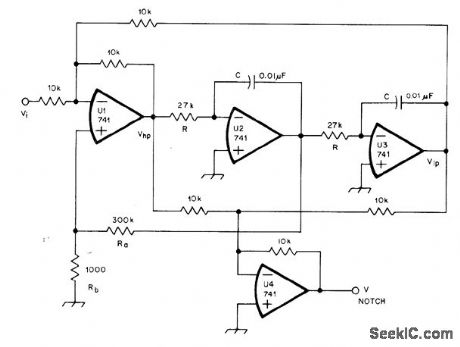
With values obtained from design equations and graph in article, state-variable or universal filter provides a of 100 with four opamps. Notch filter is achieved by adding low-pass and high-pass outputs equally, for feed to dual-input summing amplifier.M.Berlin, The State-Variable Filter,QST, April 1978, p 14-16. (View)
View full Circuit Diagram | Comments | Reading(1246)
AMPLIFIED_TTL_INTERFACE_FOR_VMOS
Published:2009/7/2 21:08:00 Author:May
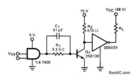
Bipolar voltage amplifier Q1 translates TTL output swing of 0.4 to 2.4 V from 7400 interface to 15V drive signal for S55V01 VMOS peripheral driver. Circuit can be driven by any low-level signal, including ECL, if comparator such as AM686 is used in place of SN7400 quad NAND gate.Switching times of circuit are less than 40 ns in both directions.-L. Shaeffer, VMOS Peripheral Drivers Solve High Power Load Interface Problems, ComputerDesign, Doc. 1977, p 90, 94, and 96-98. (View)
View full Circuit Diagram | Comments | Reading(666)
741_OPAMP
Published:2009/7/2 21:04:00 Author:May
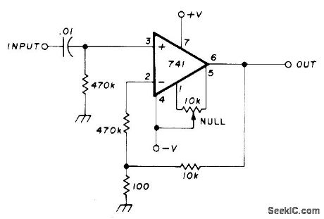
Power supply and null pot connections for TO-5 metal-can packageand 8-lead DIP package are shown. Maximum rated power supply voltages are ±18 V, but lower voltages may be used. 9-V transistor battery is often used for each supply, but higher voltages will permit larger output signal swing. Pin 3 is inverting input, and pin 4 is noninverting input.With values shown, both input terminals see about same resistance. and output offset can be nulled to zero. Gain of circuit is about l00.-C. Hall, Circuit Design with the 741 Op Amp. Ham Radio. April 1976. p 26-29. (View)
View full Circuit Diagram | Comments | Reading(1185)
175_MHz_40_W_amplifier_136_V_supynly
Published:2009/7/24 2:19:00 Author:Jessie
The electrical characteristics for the 2N3924 shown in this circuit are given in Fig.2-14B. (View)
View full Circuit Diagram | Comments | Reading(554)
TOTEM_POLE_ECL_INTERFACE_FOR_VMOS
Published:2009/7/2 21:00:00 Author:May
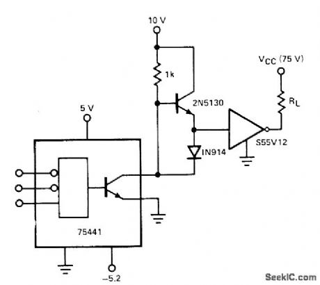
Transistor and diode in totem-pole configuration improve performance of SN75441 ECL-compatible peripheral driver for S55V12 VMOS.-L. Shaeffer, VMOS Peripheral Drivers Solve High Power Load Interface Problems, Computer Design, Dec. 1977, p 90, 94, and 96-98. (View)
View full Circuit Diagram | Comments | Reading(689)
UNITY_GAIN_AF_CURRENT_AMPLIFIER
Published:2009/7/2 20:57:00 Author:May
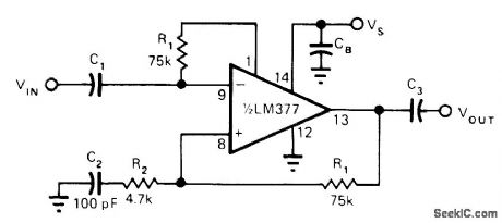
External components are used with National LM377/ 378/379 family of opamps to provide stability at unity gain. Article gives design equations. At frequencies above audio band. gain rises with frequency.to、Mell above 10 at 340 kHz forvalues shown.-D Bohn. AC Unity-Gain Power Buffers Amplify Curren. EDN Magazine. May 5.1977. p113-114. (View)
View full Circuit Diagram | Comments | Reading(721)
STORING_SINGLE_PULSE
Published:2009/7/2 20:53:00 Author:May
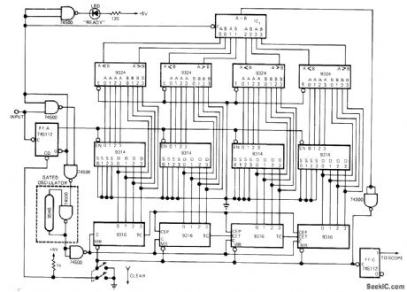
Designed to take single-event positive-going TTL pulse, occurring only once when series of logic conditions is met, and recreating pulse accurately on CRO as square wave in which half of cycle represents original pulse width. FF-A and 9316 binary counters are initially eleared. Input pulse of interest gates delay-line osciliator (lower left) on for duration of pulse width. During this time, binary representation of pulse width is accumulated in 9316 counters, then stored in 9314 D-latches. At same time, final 9324 comparator IC1 is enabled and oscillator is gated on again to reset 9316s and toggle FF-C. Square-wave output of FF-C then represents original pulse width within 35 ns (one clock).-N, L. White, Don't Miss That Single Event Pulse-Store it, EDN Magazine, Sept. 20, 1975, p 70 and 72. (View)
View full Circuit Diagram | Comments | Reading(822)
CMOS_DRIVER_FOR_OPAMP
Published:2009/7/2 20:43:00 Author:May
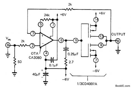
CMOS inverterpalr(one-third of CD4007A) iS used in closedloop mode as unity-gain voltage follower for CA3080 opamp .Slew rateis 1 V/μS Output current capability of 6 mA can be increased by paralleling two other sections of CMOS.-B Furlow.CMOS Gates in Linear Applications: The Results Are Surprisingly Good.EDN Magazlne.March 5.1973.p42-48. (View)
View full Circuit Diagram | Comments | Reading(929)
PEAK_SENSING_OPERATIONAL_AMPLIFIER
Published:2009/7/24 1:54:00 Author:Jessie
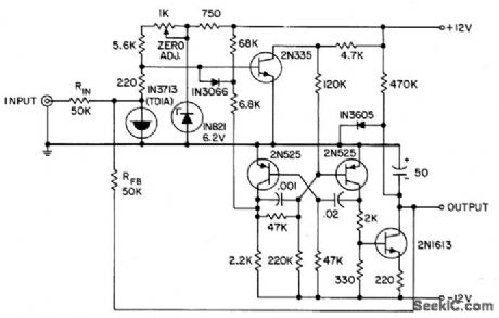
Operates as slideback sensing circuit to give d-c output that is proportional to positive peak of repetitive input signal. Will measure peaks of pulses as narrow as 1 nsec.- Transistor Manual, Seventh Edition, General Electric Co., 1964, p 371. (View)
View full Circuit Diagram | Comments | Reading(712)
SYMMETRICAL_SATURATED_FLIP_FLOP
Published:2009/7/24 1:53:00 Author:Jessie
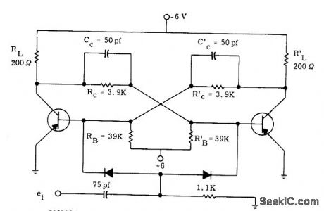
Developed for inexpensive 2N711 germanium pnp mesa switching transistors, to serve as building block for high-speed computer applications. Two or more flip4lops can be cascaded to form counter, or used as shift register by separating inputs. Close regulation is required for -6 V supply.-P. A. McInnis, Low-Cost Computer Circuits, Motorola Application Note AN-130, Nov. 1965. (View)
View full Circuit Diagram | Comments | Reading(918)
400_MHz_10_W_amplifier_28-V_supply
Published:2009/7/24 2:18:00 Author:Jessie
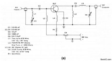
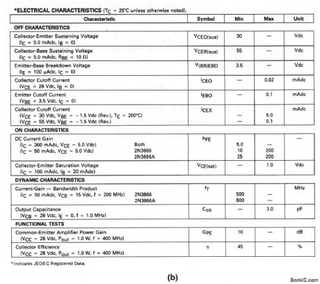
The electrical characteristics for the 2N3866 shown in this circuit are given in Fig. 2-13B. (View)
View full Circuit Diagram | Comments | Reading(1788)
450_MHz_amplifier_75-V_Supyly
Published:2009/7/24 2:14:00 Author:Jessie

The electrical characteristics for the 2N2857 shown in this circuit are given in Fig.2-11B (View)
View full Circuit Diagram | Comments | Reading(620)
RE_IF_amplifiers
Published:2009/7/24 2:08:00 Author:Jessie
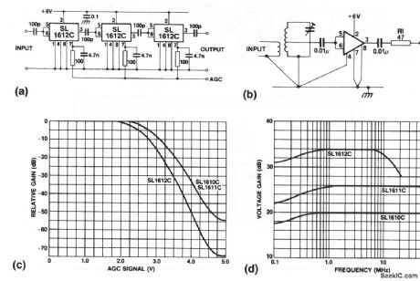
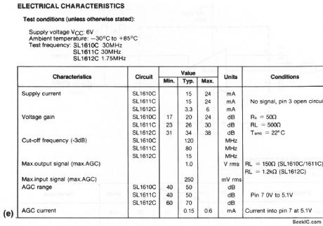
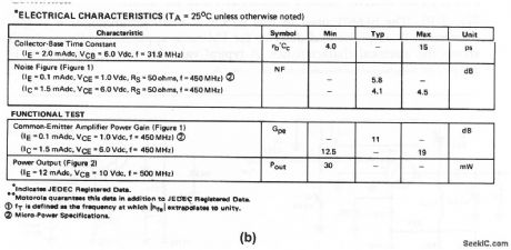
The SL1610, SL1611, and SL1612 shown in these circuits are RF voltage amplifiers with AGC provisions. The voltage gains are 10, 20, and 50, respectively, and the upper frequency response varies from 15 to 120 MHz, according to the type. Figure 2-8A shows three SL1612Cs connected as an IF amplifier(with AGC). Figure 2-8B shows any of the three ICs connected as an RF amplifier (without AGC). Figures 2-8C and 2-8D show the AGC characteristics and gain versus frequency, respectively, for the three ICs. Electrical characteristics are shown in Fig. 2-8E. (View)
View full Circuit Diagram | Comments | Reading(924)
POSTAMPLIFIER_FOR_OPAMP
Published:2009/7/2 8:38:00 Author:May
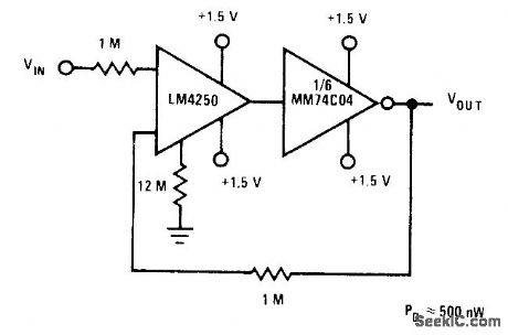
High input impedance of National MM74CO4 invertermakes it ideal for isolating load from output of LM425O micropower opamp operating from single dry cell- Linear Applications.vol.2. National Semiconductor. Santa Clara.CA. 1976,AN-88.p2 (View)
View full Circuit Diagram | Comments | Reading(582)
BUFFERED_OPAMP
Published:2009/7/2 8:03:00 Author:May
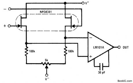
NPD8301 dual FET is ideal low-offset low-drift buffer for LM101A opamp. Matched sections of FET track well over entire bias range, for improved common-mode re jec-ion.- FET Databook. National Semiconductor. Santa Clara. CA. 1977. p 6-26-6-36. (View)
View full Circuit Diagram | Comments | Reading(1019)
Wideband_AGC_amplifier
Published:2009/7/24 2:10:00 Author:Jessie
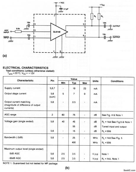
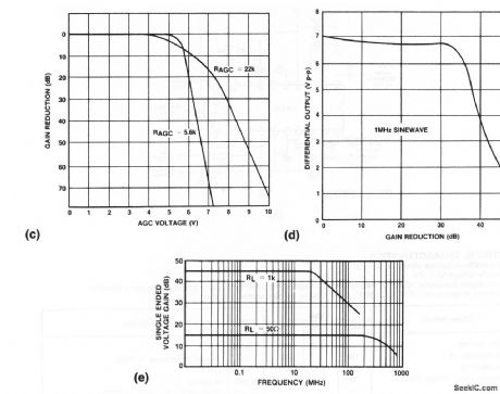
The SL640 shown in this circuit is a broadband amplifier, providing over 15 dB of linear gain into 50Ω at 400 MHz.Figure 2-9B shows the electrical characteristics. Figures 2-9C, 2-9D,and 2-9E show AGC characteristics, differential output, and single-ended voltage gain, respectively. (View)
View full Circuit Diagram | Comments | Reading(0)
175_MHz_25_W_amplifier_28_V_supply
Published:2009/7/24 2:16:00 Author:Jessie


The electrical characteristics for the 2N3553 shown in this circuit are given in Fig. 2-12B. (View)
View full Circuit Diagram | Comments | Reading(1501)
PULSE_COMPLETING_SCHMITT
Published:2009/7/2 4:55:00 Author:May
Half of 7413 dual four-input NAND Schmitt trigger forms RS bistable which ensures that cycle is completed after switch is opened. Low-impedance exponential sawtooth output is produced at point C.Point A is high when oscillator is running and can be used as control signaL-T. P. Hopkins, Improved Schmitt Trigger Oscillator, Wireless World, Jan. 1978, p 58. (View)
View full Circuit Diagram | Comments | Reading(1300)
175_MHz_10_W_amplifier_12_V_supply
Published:2009/7/24 2:21:00 Author:Jessie
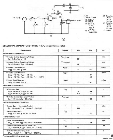
The electrical characteristics for the 2N4427 shown in this given in Fig.2-16B. (View)
View full Circuit Diagram | Comments | Reading(558)
| Pages:129/250 At 20121122123124125126127128129130131132133134135136137138139140Under 20 |
Circuit Categories
power supply circuit
Amplifier Circuit
Basic Circuit
LED and Light Circuit
Sensor Circuit
Signal Processing
Electrical Equipment Circuit
Control Circuit
Remote Control Circuit
A/D-D/A Converter Circuit
Audio Circuit
Measuring and Test Circuit
Communication Circuit
Computer-Related Circuit
555 Circuit
Automotive Circuit
Repairing Circuit