
Amplifier Circuit
Index 130
BALANCE_AND_LOUDNESS_AMPLIFIER
Published:2009/7/2 4:40:00 Author:May
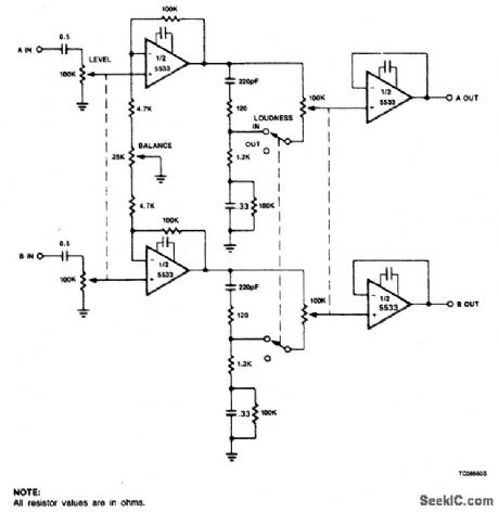
The circuit shows a combination of balance and loudness controls. Due to the non-linearity of the human hearing system, the low frequencies must be boosted at low listening levels. Balance, level, and loudness controls provide all the listening controls to produce the desired music response. (View)
View full Circuit Diagram | Comments | Reading(1824)
VOLUME,BALANCE,LOUDNESS&POWER_AMPS
Published:2009/7/2 4:39:00 Author:May
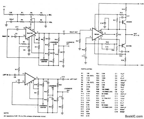
This circuit should prove suitable as a design example for audio sound application. (View)
View full Circuit Diagram | Comments | Reading(665)
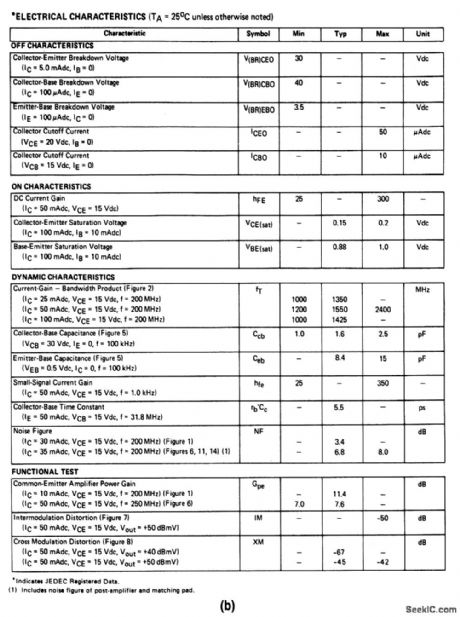
400_MHz_10_W_amplifier_136_V_supply
Published:2009/7/24 2:20:00 Author:Jessie
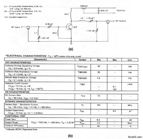
The electrical characteristics for the 2N3948 shown in this circuit are given in Fig. 2-15B. (View)
View full Circuit Diagram | Comments | Reading(657)
MICROPHONE_PREAMPLIFIER
Published:2009/7/2 4:38:00 Author:May
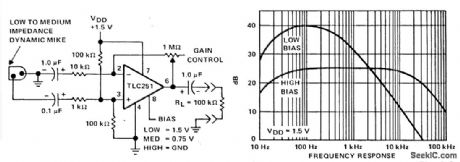
A microphone preamplifier using a :om CM0S op amp complete with its own battery, is small enough to be put in a small mike case. The amplifier operates from a 1.5-V mercury cell battery at low supply currents. This preamplifier will operate at very low power levels and maintain a reasonable frequency response as well. The TLC251 operated in the low bias mode (operating at 1.5 V) draws a supply current of only 10 μA and has a -3 dB frequency response of 27 Hz to 4.8 kHz. With pin 8 grounded, which is designated as the high bias condition, the upper limit increases to 25 kHz. Supply current is only 30 μA under those conditions. (View)
View full Circuit Diagram | Comments | Reading(1214)
STEREO_PREAMPLIFIER_1
Published:2009/7/2 4:37:00 Author:May
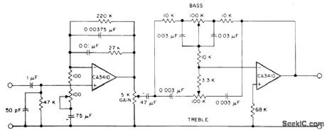
This circuit has RIAA playback equalization, tone controls, and adequate gain to drive a majority of commercial power amplifiers, using the CA3410 BiMOS op amp. Total harmonic distortion, when driven to provide a 6-V output, is less than 0.035% in the audio-frequency range of 150 Hz to 40 kHz. Complete stereo preamplifier consists of duplicating this circuit using the two remaining CA3410 amplifiers. (View)
View full Circuit Diagram | Comments | Reading(870)
AUDIO_COMPRESSOR
Published:2009/7/2 4:35:00 Author:May
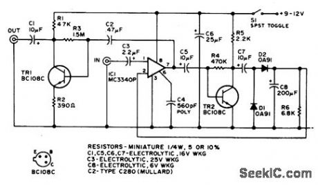
A MC3340P is used as a variable gain amplifier. The output of TR2 is rectified and controls the gain of IC1. (View)
View full Circuit Diagram | Comments | Reading(1877)
STEREO_PREAMPLIFIER
Published:2009/7/2 4:33:00 Author:May
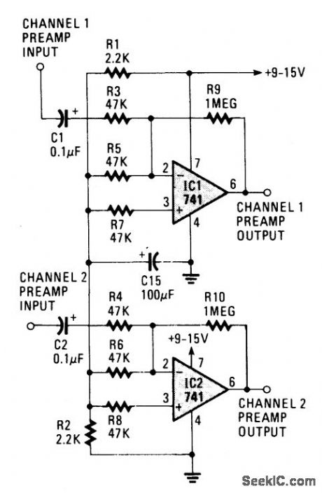
The circuit provides better than 20-dB gain in each channel. A better op-amp type will give a better noise figure and bandpass. In this circuit the roll-off is acute at 20,000 Hertz. (View)
View full Circuit Diagram | Comments | Reading(0)
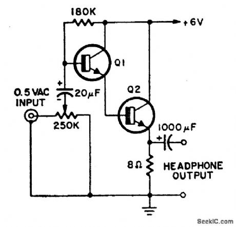
TRANSISTOR_HEADPHONE_AMPLIFIER
Published:2009/7/2 4:31:00 Author:May
View full Circuit Diagram | Comments | Reading(1021)
AUDIO_DISTRIBUTION_AMPLIFIER
Published:2009/7/2 4:24:00 Author:May
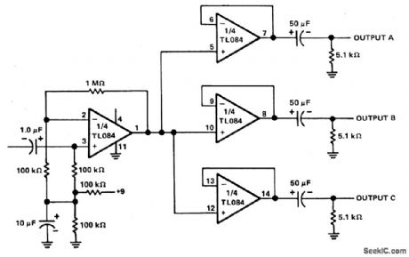
The three channel output distribution amplifier uses a single TL084. The first stage is capacitively coupled with a 1.0 μF electrolytic capacitor. The inputs are at 1/2 VCC rail or 4.5 V. This makes it possible to use a single 9 V supply. A voltage gain of 10 (1 M ohm/100 k ohm) is obtained in the first stage, and the other three stages are connected as unity-gain voltage followers. Each output stage independently drives an amplifier through the 50 μF output capacitor to the 5.1 k ohm load resistor. The response is flat from 10 Hz to 30 kHz. (View)
View full Circuit Diagram | Comments | Reading(0)
SOUND_MIXER_AMPLIFIER
Published:2009/7/2 4:19:00 Author:May
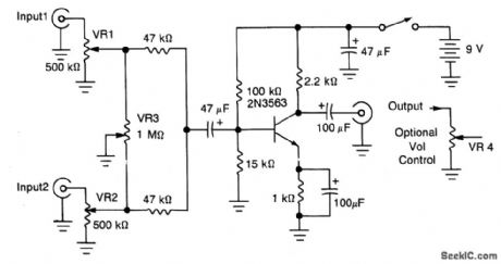
Both input signals can be independently controlled by VR1 and VR2. The balance control VR3 is used to fade out one signal while simultaneously fading in the other. The transistor provides gain and the combined output signal level is controlled by VR4 (optional). (View)
View full Circuit Diagram | Comments | Reading(785)
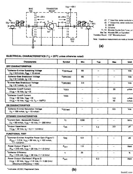
500_MHz_075_W_amplifier_28-V_supply
Published:2009/7/24 2:22:00 Author:Jessie
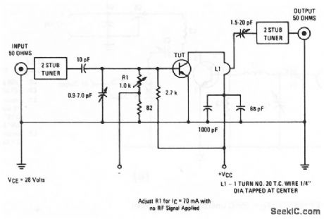
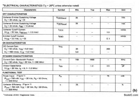
The electrical characteristics for the 2N4428 shown in this circuit are given in Fig.2-17B. (View)
View full Circuit Diagram | Comments | Reading(702)
X100_instrumentation_amplifier
Published:2009/7/24 3:08:00 Author:Jessie
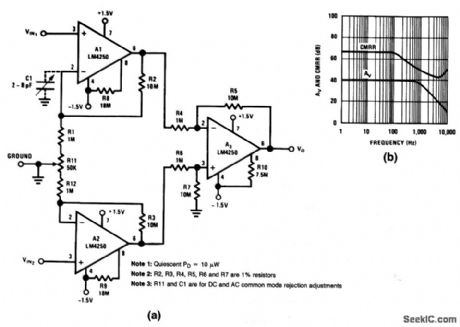
This circuit requires two 1.5-V cells connected directly (no power switch) to the V+ and V- terminals. Total current drain is 2.8 μA. R11 matches gains of Al and A2 to get maximum common-mode rejection ratio. Figure 8-32B shows both CMRR and voltage gain across frequency range. C1 balances wiring (rather than amplifier frequency response) to give an additional 10 to 20 dB of CMRR. Maximum peak-to-peak output into a 100-kΩ load is about 1.8 V. When doing power measurements on this circuit, remember that even a 1-MΩ scope probe placed between +1.5 V and -1.5 V more than doubles the power drawn from the batteries. (View)
View full Circuit Diagram | Comments | Reading(922)
225_to_400_MHz_60_W_broadband_amplifier_28_V_supply
Published:2009/7/24 3:07:00 Author:Jessie
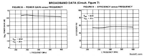
The electrical characteristics for the 2N6439 shown in this circuit are given in Fig.2-39B. (View)
View full Circuit Diagram | Comments | Reading(708)
200_MHz_narrowband_amplifier_15_V_supply
Published:2009/7/24 2:49:00 Author:Jessie
The electrical characteristics for the 2N5943 shown in this circuit are given in Fig. 2-31B. (View)
View full Circuit Diagram | Comments | Reading(839)
10_AMP_REGULATOR_WITH_CURRENT_AND_THERMAL_PROTECTION
Published:2009/7/2 3:50:00 Author:May
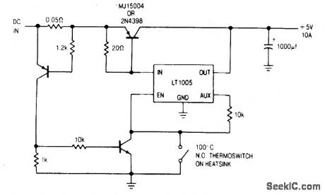
View full Circuit Diagram | Comments | Reading(1303)
ARIABLE_CURRENT_SOURCE,100_mA_TO_2_AMP
Published:2009/7/2 3:24:00 Author:May
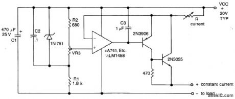
Circuit NotesThe output current is set by the resistor R in the collector of Tr2, which may be varied to offer a range of output currents from 100 mA to 2 A with fine control by means of VR3 which varies the reference voltage to the non-inverting input of the op amp. The feedback path from the output to the inverting input of the op amp maintains a constant voltage across R, equal to(VCC-VIN)/and hence a constant current to the load given by(VCC-VIN)/R. (View)
View full Circuit Diagram | Comments | Reading(693)
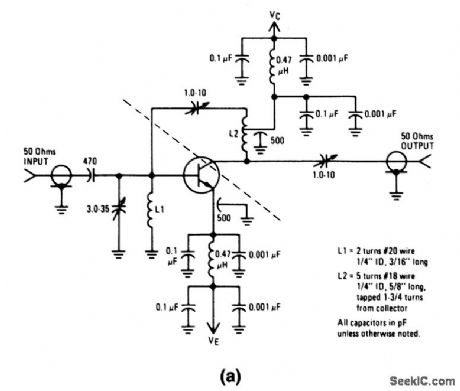
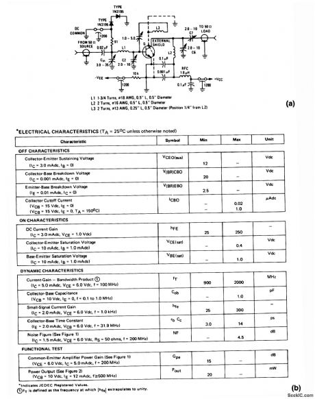
216_MHz_high_gain_amplifier_15-V_supply
Published:2009/7/24 2:32:00 Author:Jessie
The electrical characteristics for the 2N5019 shown in this circuit are given in Fig.2-22B. (View)
View full Circuit Diagram | Comments | Reading(565)
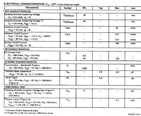
1_GHz_10-W_amplifier_28-V_supply
Published:2009/7/24 2:30:00 Author:Jessie
The electrical characteristics for the 2N5108 shown in this circuit are given in Fig 2-20B. (View)
View full Circuit Diagram | Comments | Reading(549)
175_MHz_70_W_amplifier_28_V_supply
Published:2009/7/24 2:39:00 Author:Jessie

The electrical characteristics for the 2N5641 shown in this circuit are given in Fig. 2-26B. (View)
View full Circuit Diagram | Comments | Reading(1615)
200_MHz_high_gain_amplifier_6_V_supply
Published:2009/7/24 2:37:00 Author:Jessie
The electrical characteristics for the 2N5179 shown in this circuit are given in Fig.2-24B. (View)
View full Circuit Diagram | Comments | Reading(618)
| Pages:130/250 At 20121122123124125126127128129130131132133134135136137138139140Under 20 |
Circuit Categories
power supply circuit
Amplifier Circuit
Basic Circuit
LED and Light Circuit
Sensor Circuit
Signal Processing
Electrical Equipment Circuit
Control Circuit
Remote Control Circuit
A/D-D/A Converter Circuit
Audio Circuit
Measuring and Test Circuit
Communication Circuit
Computer-Related Circuit
555 Circuit
Automotive Circuit
Repairing Circuit