
Amplifier Circuit
Index 131
50_MHz_40-W_amplifier_125_V_supply
Published:2009/7/24 2:44:00 Author:Jessie
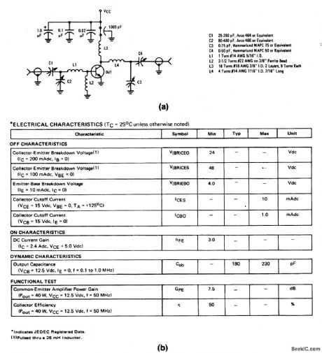
The electrical characteristics for the 2N5849 shown in this circuit are given in Fig.2-29B (View)
View full Circuit Diagram | Comments | Reading(779)
175_MHz_40_W_amplifier_28_V_supply
Published:2009/7/24 2:42:00 Author:Jessie
The electrical characteristics for the 2N5643 shown in this circuit are given in Fig. 2-28B. (View)
View full Circuit Diagram | Comments | Reading(1002)
175_MHz_20_W_amplifier_28_V_supply
Published:2009/7/24 2:42:00 Author:Jessie

The electrical characteristics for the 2N5642 shown in this circuit are given in Fig. 2-27B. (View)
View full Circuit Diagram | Comments | Reading(889)
AF_POWERED_CLIPPER
Published:2009/7/2 1:56:00 Author:May
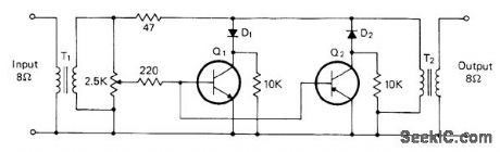
Designed for use just ahead of 8-ohm loudspeaker in receiver covering lower amateur phone bands (75 and 40 me-ters). Reduces hissing noise caused by shortwave diathermy, electric motors, and fluorescent lighting, as well as impulse noise generated by auto ignition system or atmospheric interference. T1 and T2 are transistor radio output transformers with 500:4 or 600:8 ohm impedance. Q1 is 2N2222 NPN transistor. Q2 is 2N29O7 PNP transistor. D1 and D2 are 1N270.-C. Laster. An Audio Powered Noise Clipper. CQ. May 1976. p 26-27. (View)
View full Circuit Diagram | Comments | Reading(2500)
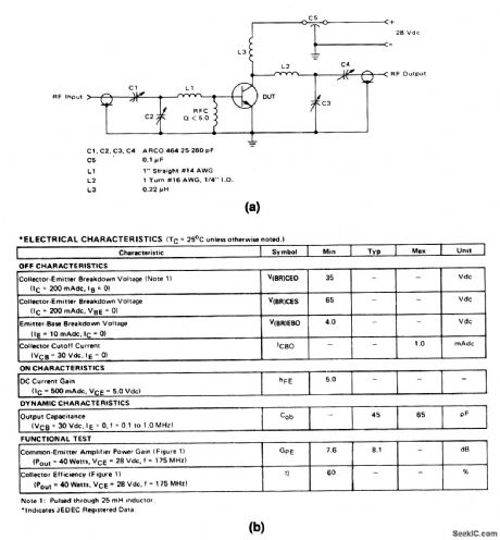
175_MHz_25_W_amplifter_125_V_supply
Published:2009/7/24 2:58:00 Author:Jessie
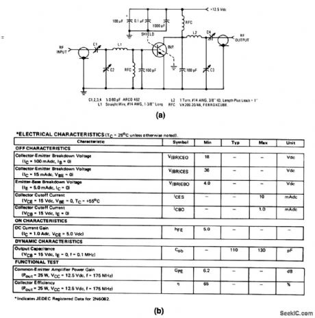
The electrical characteristics for the 2N6082 shown in this circuit are given in Fig.2-35B. (View)
View full Circuit Diagram | Comments | Reading(1901)
175_MHz_15_W_amplifier_125_V_supply
Published:2009/7/24 2:56:00 Author:Jessie

The electrical characteristics for the 2N6081/MRF221 shown in this circuit are given in Fig.2-34B. (View)
View full Circuit Diagram | Comments | Reading(1311)
POWER_AMPLIFIER
Published:2009/7/2 1:23:00 Author:May

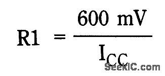

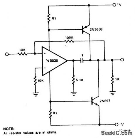
Circuit NotesFor most applications, the available power from op amps is sufficient. There are times when more power handling capability is necessary. A simple power booster capable of driving moderate loads uses an NE5535 device. Other amplifiers may be substituted only if R1 values are changed because of the ICC current required by the amplifier.R1 should be calculated from the expression (View)
View full Circuit Diagram | Comments | Reading(1965)
440__to_480_MHz_broadband_UHF_amplifier_125_V_supply
Published:2009/7/24 2:54:00 Author:Jessie

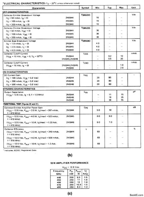
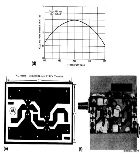
The electrical characteristics for the 2N5944 and 2N5946 shown in this circuit are given in Fig. 2-33B. Figures 2-33C and 2-33D show the amplifier performance over the frequency range. Figures 2-33E and 2-33F show the PC-board photomaster, and parts placement, respectively. Those not familiar with microstrip techniques (for Z1, Z2, and Z3) should read the many Motorola Publications, such as AN548A and AN555. (View)
View full Circuit Diagram | Comments | Reading(1174)
90_W_AUDIO_POWER_AMPLIFIER_WITH_SAFE_AREA_PROTECTION
Published:2009/7/2 1:20:00 Author:May
View full Circuit Diagram | Comments | Reading(933)
250_MHz_broadband_amplifier_15_V_supply
Published:2009/7/24 2:51:00 Author:Jessie

The electrical characteristics for the 2N5943 shown in this circuit are given in Fig. 2-31B. (View)
View full Circuit Diagram | Comments | Reading(777)
AUDIBLE_VISIBLE_METRONOME
Published:2009/7/2 1:19:00 Author:May
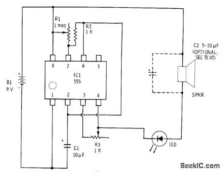
Produces uniformly spaced beats in synchronism with flashes of LED, at rate that can be adiusted with R1 from one beat every few seconds to ten or more beats per second. Use red Radio Shack 276-041 or similar LED. Add switch in series with battery to avoid disturbing setting of R1. R3 serves as volume control. Add 5-10 μF capacitor across loudspeaker to mellow beat sound if desired.-F. M. Mims. Electronic.'' Music Projects. Vol. 1. Radio Shack, Fort Worth, TX, 1977, 2nd Ed.p 55-59. (View)
View full Circuit Diagram | Comments | Reading(763)
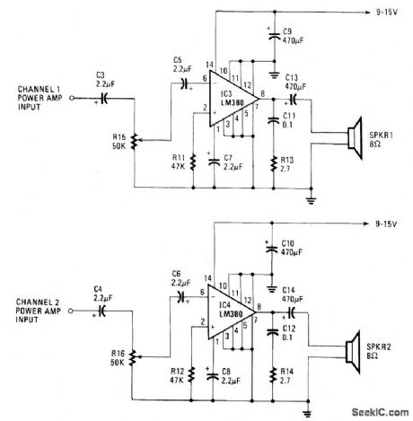
REAR_SPEAκER_AMBIENCE(4_CHANNEL)AMPLIFIER
Published:2009/7/2 1:13:00 Author:May

Circuit Notes
Rear channel ambience can be added to an existing stereo system to extract a difference signal(R-L or L-R)which, when combined with some direct signal(R or L), adds fullness, or concert hall realism to the reproduction of recorded music. Very little power is required at the rear channels, hence an LM1877 suffices for most ambience applications. The inputs are merely connected to the existing speaker output terminals of a stereo set, and two more speakers are connected to the ambience circuit outputs. The rear speakers should be connected in the opposite phase to those of the front speakers, as indicated by the +/- signs. (View)
View full Circuit Diagram | Comments | Reading(998)
PREAMP_FOR_ACOUSTIC_PiCkUP
Published:2009/7/2 1:12:00 Author:May
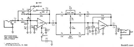
National LM387 dual opamp provides switchable gain choice of ±10 dB along with bass/treble tone control and volume control. Used with flat-response piezoceramic contact pickup for acoustic stringed musical instruments such as guitar.violin. and dulcimer. Half of IC is used as controllable gain stage, and other half is used as active two-band tone-control block.- Audio Handbook. National Semiconductor. Santa Clara. CA. 1977. p 5-12. (View)
View full Circuit Diagram | Comments | Reading(3552)
WALKMAN_AMPLIFIER
Published:2009/7/2 1:08:00 Author:May
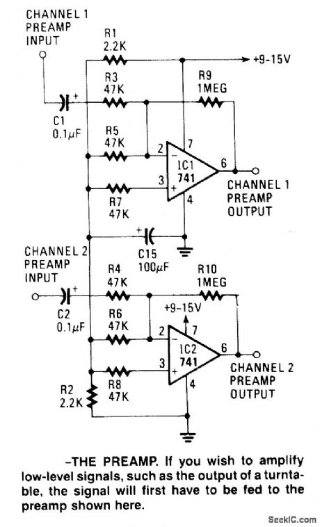
Circuit Notes
The gain of the low-cost IC is internally fixed so that it is not less than 34 dB(50 times). A unique input stage allows input signals to be referenced to ground. The output is automatically self centering to one half the supply voltage. The output is also short-circuit proof with internal thermal limiting. With a maximum supply of 15 volts and an 8 ohm load, the output is around 1.5 watts per channel. The input stage is usable with signals from 50 mV to 500 mV rms. If the amplifier is to be used with a source other than a personal stereo, such as a phonograph or an electric guitar, some type of preamplifier is required. A suitable circuit is shown. In that circuit, two 741 op amps have been configured as input amplifiers. Their input stages referenced to a common point-half the supply voltage. That voltage is derived from a voltage divider made up of RI and R2, two 2.2 k resistors. The gain of each of the 741's has been fixed at 21 by the input resistors(R9, R10). Input capacitors, C1 and C2, are used to filter out any dc component from the input signal. (View)
View full Circuit Diagram | Comments | Reading(2570)
LOW_POWER_AUDIO_AMPLIFIER
Published:2009/7/2 0:46:00 Author:May
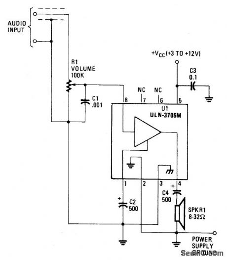
Circuit Notes
The amplifier operates from supplies ranging up to 12 volts, and operates(with reduced volume)from supply voltages as low as 1.8 volts without having distortion rise to unacceptable levels.(Its power requirements make it suitable for solar-cell application.)Components external to the integrated circuit, U1, consist of four capacitors and a potentiometer for volume control. Capacitor C3 is for decoupling, low-frequency roll-off, and power-supply ripple rejection. Capacitor C4 is an electrolytic type that couples the audio output to an 8 to 32 ohm speaker that is efficient. (View)
View full Circuit Diagram | Comments | Reading(782)
BULL_HORN
Published:2009/7/2 0:42:00 Author:May
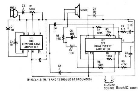
Circuit Notes
The input audio signal is fed to pin 3 of U1, an LM386 low-voltage amplifter, via C3 and R1. Potentiometer R1 sets the drive or volume level. U1, which serves as a driver stage, can be set for a gain of from 20 to 200. The output of U1 at pin 5 is fed to U2-a 377 dual two-watt amplifier connected in parallel to produce about four watts of output power-at pins 6 and 9 via C4 and C5. Frequency stability is determined by R2, R4, and C10 on one side, and the corresponding components R6, R5, and C9 on the other side. The outputs of the two amplifiers (at pins 2 and 13) are capacitively coupled to SPKR1 through C6 and C7. (View)
View full Circuit Diagram | Comments | Reading(2)
AUDIO_POWER_AMPLIFIER
Published:2009/7/2 0:40:00 Author:May
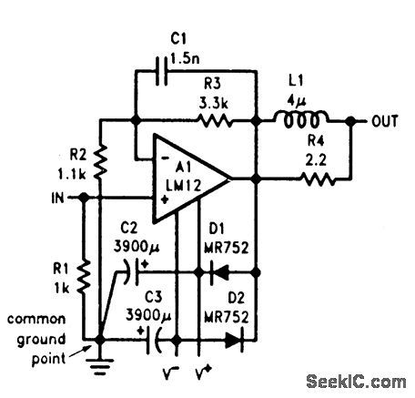
Circuit Notes
Output-clamp diodes are mandatory because loudspeakers are inductive loads. Output LR isolation is also used because audio amplifiers are usually expected to handle up to 2 μF load capacitance. Large, supply-bypass capacitors located close to the IC are used so that the rectifted load current in the supply leads does not get back into the amplifier, increasing high-frequency distortion. Single-point ground-ing for all intemal leads plus the signal source and load is recommended to avoid ground loops that can increase distortion. (View)
View full Circuit Diagram | Comments | Reading(0)
2_TO_6_W_AUDIO_AMPLIFIER_WITH_PREAMPLIFIER
Published:2009/7/2 0:38:00 Author:May

Circuit NotesThe monolithic integrated audio amplifier circuit is especially designed for portable radio and recorder applications and delivers up to 4 W in a 4 ohm load impedance. (View)
View full Circuit Diagram | Comments | Reading(641)
BASIC_UJT_ORGAN
Published:2009/7/2 0:38:00 Author:May
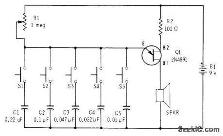
Switches give choice of five audio frequencies for simple transistor oscillator driving loudspeaker. Adiust R1 for best combination of sounds. Capacitorvalues can be changed to give other frequencies. Ideal for classroom demonstrations.-F. M. Mims. Electronic Music Projects. Vol. Radio Shack. Fort Worth. TX. 1977. 2nd Ed., p 37-43. (View)
View full Circuit Diagram | Comments | Reading(1279)
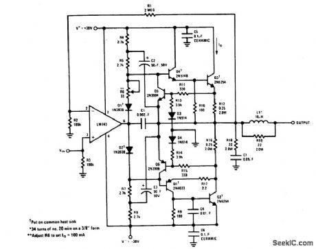
25_WATT_AMPLIFIER
Published:2009/7/2 0:36:00 Author:May
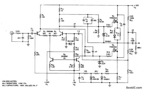
Transistors are used for current sources.Base drive for these transistors is de-rived from the main power supply VA, so that their collector current is proportional to the rail voltage. This feature holds the voltage on the diff-amp collectors close to VA/2.The sensitivity of IQ to VA is about 3.4 mA/volt when Vg is held constant; the sensitivity of IQ to VB is -15 mA/volt when VA is held constant. In a practical amplifier with a non-regulated supply, variations in power output will cause fluctuations in VA, but will not affect Vg; therefore, having IQ increase slightly with power output will tend to compensate for the 3.4 mA/volt IQVA sensitivity. In the case of line voltage variations, since VA is about five times Vg, the sensitivities tend to cancel, leaving a net sensitivity of about 2 mA/volt. (View)
View full Circuit Diagram | Comments | Reading(851)
| Pages:131/250 At 20121122123124125126127128129130131132133134135136137138139140Under 20 |
Circuit Categories
power supply circuit
Amplifier Circuit
Basic Circuit
LED and Light Circuit
Sensor Circuit
Signal Processing
Electrical Equipment Circuit
Control Circuit
Remote Control Circuit
A/D-D/A Converter Circuit
Audio Circuit
Measuring and Test Circuit
Communication Circuit
Computer-Related Circuit
555 Circuit
Automotive Circuit
Repairing Circuit