
Amplifier Circuit
Index 140
Silicon Controlled Trigger Circuit
Published:2011/7/21 9:08:00 Author:Joyce | Keyword: Silicon Controlled, Trigger
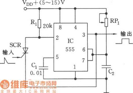
As shown in the figure, 555, R1, RP1, C2 and some other components constitute the trigger delay circuit. Commonly, 555 is in the state of reset , and feet 3 displays a low level since R1 is connected with VDD; When triggered signals come in , SCR will break over ,feet 2 will have a low level signal which will turn 555 to output a high level. The temporary stable width is: τ = 1.1 RP1C2 . After triggering, SCR will shut off. This circuit can lower the requirement of triggering pulse. If CMOS type 555 (or 556) is used, the triggering current can also be reduced. (View)
View full Circuit Diagram | Comments | Reading(754)
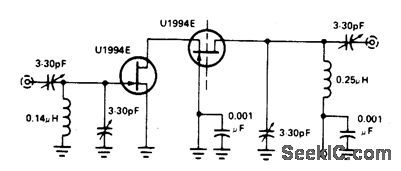
450_MHz_COMMON_SOURCE_AMPLIFIER
Published:2009/6/29 4:26:00 Author:May
View full Circuit Diagram | Comments | Reading(679)
High Frequency Thyristor Trigger Circuit
Published:2011/7/21 9:16:00 Author:Joyce | Keyword: High Frequency , Thyristor , Trigger
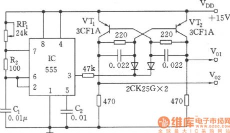
As shown in the figure, 555 ,RP1, R2, C1 constitute the astable multivibrator.The oscillation frequency and duty ratio can be altered by adjusting RP1. The output pulse will trigger the flip-flop composed of VT1 and VT2. V01, V02 can trigger two thyristors alternatively .
(View)
View full Circuit Diagram | Comments | Reading(1539)
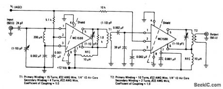
200_MHz_NEUTRALIZED_COMMON_SOURCE_AMPLIFIER
Published:2009/6/29 4:26:00 Author:May
View full Circuit Diagram | Comments | Reading(578)
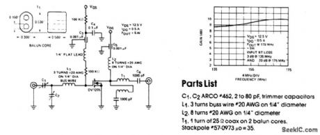
80_MHz_CASCODE_AMPLIFIER
Published:2009/6/29 4:25:00 Author:May
View full Circuit Diagram | Comments | Reading(1072)
TWO_METER_AMPLIFIER5_W_OUTPUT
Published:2009/6/29 4:24:00 Author:May
View full Circuit Diagram | Comments | Reading(622)
30_MHz_AMPLIFIER_POWER_GAIN=50_dBBW≈10_MHz
Published:2009/6/29 4:23:00 Author:May
View full Circuit Diagram | Comments | Reading(482)
60_MHz_AMPLIFIER
Published:2009/6/29 4:23:00 Author:May
View full Circuit Diagram | Comments | Reading(614)
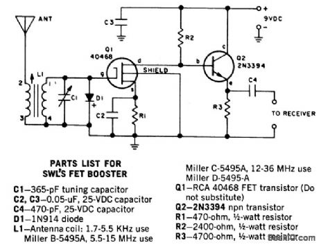
TRANSISTORIZED_Q_MULTIPLIER_FOR_USE_WITH_IFS_IN_THE_1400_kHz_RANGE
Published:2009/6/29 4:21:00 Author:May
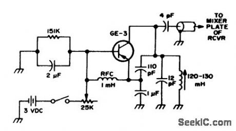
View full Circuit Diagram | Comments | Reading(839)
UHF_AMPLIFIER_WITH_INVERTING_GAIN_OF_2_AND_LAG_LEAD_COMPENSATIONGAIN_BANDWIDTH_PRODUCT_350_MHz
Published:2009/6/29 4:20:00 Author:May
View full Circuit Diagram | Comments | Reading(827)
ULTRA_HIGH_FREQUENCY_AMPLIFIER
Published:2009/6/29 4:19:00 Author:May
View full Circuit Diagram | Comments | Reading(719)
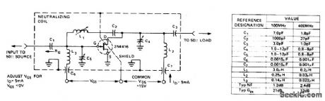
100_MHz_AND_400_MHz_NEUTRALIZED_COMMON_SOURCE_AMPLIFIER
Published:2009/6/29 4:18:00 Author:May
View full Circuit Diagram | Comments | Reading(650)
135_175_MHz_AMPLIFIER
Published:2009/6/29 4:16:00 Author:May
View full Circuit Diagram | Comments | Reading(638)
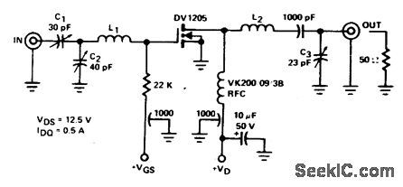
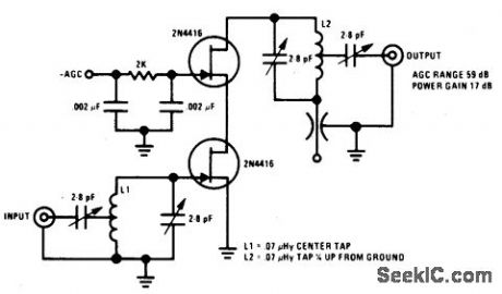
200_MHz_CASCODE_AMPLIFIER
Published:2009/6/29 4:15:00 Author:May
This 200 MHz JFET cascode circuit features low cross-modulation, large signal handling ability, no neutralization, and AGO controlled by biasing the upper cascade JFET. The only special requirement of this circuit is that bss of the upper unit must be greater than that of the lower unit. (View)
View full Circuit Diagram | Comments | Reading(1167)
28_V_WIDEBAND_AMPLIFIER3_to_100_MHz
Published:2009/6/29 4:14:00 Author:May
View full Circuit Diagram | Comments | Reading(689)
TWO_STAGE_60_MHz_IF_AMPLIFIER_POWER_GAIN≈80_dB_BW≈15_MHz
Published:2009/6/29 4:13:00 Author:May
View full Circuit Diagram | Comments | Reading(609)
TWO_METER_lO_WATT_POWER_AMPLIFIER
Published:2009/6/29 4:12:00 Author:May
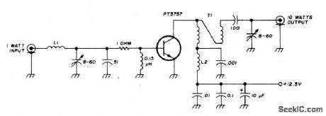
This 10-watt, 144-MHz power amplifier uses a TRW PT5757 transistor. L1 is 4 turns of no. 20 enameled, 3/32 ID; L2 is 10 turns of no. 20 enameled, 3/32 ID. Transformer T1 is a 4:1 transmission-line transformer made from a 3 length of twisted pair of no. 20 enameled wire. (View)
View full Circuit Diagram | Comments | Reading(1105)
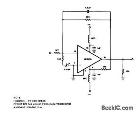
LOW_NOISE_BROADBAND_AMPLIFIER
Published:2009/6/29 4:11:00 Author:May
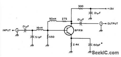
The amplifier provides 10 dB of gain from 10-600 MHz and has a 1.5-to-1 match at 50 ohms. The BFR91 has a 1.5 dB noise figures at J, 500 MHz. The circuit requires 13.5 Vdc at about 13 mA. Keep the leads on the 150 pF emitter bypass capacitor as short as possible.The 16 nH coil is 2.5 tums of #26 enamel wire on the shank of a #40 drill. The 93 nH inductor is 10 tums of the same material. (View)
View full Circuit Diagram | Comments | Reading(5452)
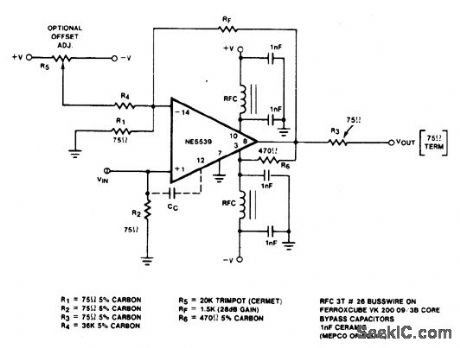
LOW_NOISE_30_MHz_PREAMPLIFIER
Published:2009/6/29 4:10:00 Author:May
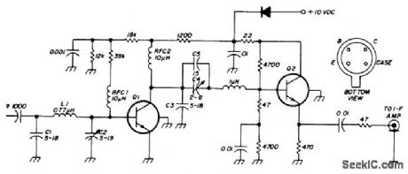
Low-noise preamplifier has a noise figure of 1.1 dB at 30 MHz and 3 dB bandwidth of 10 MHz. Gain is 19 dB. Total current drain with a +10 volt supply is 13 mA. All resistors are 1/4 watt carbon; bypass capacitors are 50-volt ceramics. (View)
View full Circuit Diagram | Comments | Reading(1260)
Op_amp_differentictl_input_instrumentation_amplifier
Published:2009/7/24 22:45:00 Author:Jessie
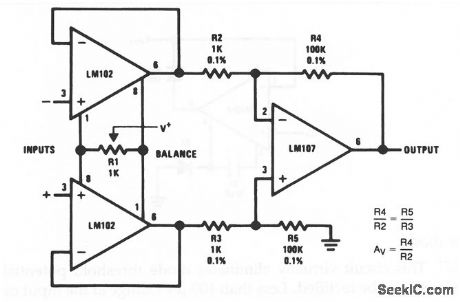
This is the op-amp version of the classic instrumentation amplifier.The circuit provides 10-V output for a 100-mW input, with gain set by the ratio of R4/R2 and R5/R3, while rejecting ±11V of common-mode noise. With both inputs grounded, R1 is adjusted until the output is zero. (View)
View full Circuit Diagram | Comments | Reading(858)
| Pages:140/250 At 20121122123124125126127128129130131132133134135136137138139140Under 20 |
Circuit Categories
power supply circuit
Amplifier Circuit
Basic Circuit
LED and Light Circuit
Sensor Circuit
Signal Processing
Electrical Equipment Circuit
Control Circuit
Remote Control Circuit
A/D-D/A Converter Circuit
Audio Circuit
Measuring and Test Circuit
Communication Circuit
Computer-Related Circuit
555 Circuit
Automotive Circuit
Repairing Circuit