
Amplifier Circuit
Index 139
Inverting_amplifier_with_high_input_impedance
Published:2009/7/24 21:13:00 Author:Jessie
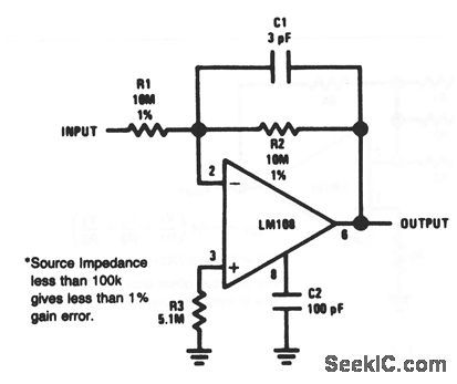
This circuit provides an input impedance of about 10 MΩ. C1 is necessary to provide stabilization feedback. C2 compensates for frequency shift caused by C1. (View)
View full Circuit Diagram | Comments | Reading(872)
Noninverting_summing_amplifier
Published:2009/7/24 21:12:00 Author:Jessie
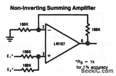
This circuit shows an LM107 in the classic noninverting summing-amplifier configuration, where VOUT depends on the sum of the input voltages (E1, E2), with all resistors at the same value. The accuracy of the circuit depends on the input-voltage source resistance (and will be 1% if the source is 1 kΩ). (View)
View full Circuit Diagram | Comments | Reading(1144)
Inverting_summing_amplifier
Published:2009/7/24 21:11:00 Author:Jessie
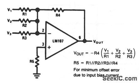
This circuit shows an LM107 in the classic inverting summing amplifier configuration, where VOUT depends on the sum of the input voltages(V1,V2,V3), as well as the ratios of R1 through R4. As shown, offset error is minimum when R5 equals the parallel resistance of R1 through R4. (View)
View full Circuit Diagram | Comments | Reading(0)
Difference_amplifier
Published:2009/7/24 21:09:00 Author:Jessie
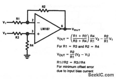
This circuit shows an LM107 in the classic difference-amplifier configuration, where VOUT depends on the difference between V1 and V2, as well as the ratios of R1 through R4. As shown, the calculations for VOUT are simplified when R1=R3 and R2=R4. (View)
View full Circuit Diagram | Comments | Reading(0)
Finger Touch Induction Switch Circuit
Published:2011/7/21 10:06:00 Author:Joyce | Keyword: Finger , Touch , Induction, Switch
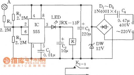
As shown in the figure, this circuit is composed of a depressurization and rectification circuit and a 555 trigger. When a hand touches the metal A, the induction signal will turn the comparator within 555 to set, K will be actuated and contact K1-1 will close; another trigger of A will release K and, disconnect K1-1. (View)
View full Circuit Diagram | Comments | Reading(1183)
One-button Biostable Switch Circuit
Published:2011/7/21 10:21:00 Author:Joyce | Keyword: One-button , Biostable , Switch
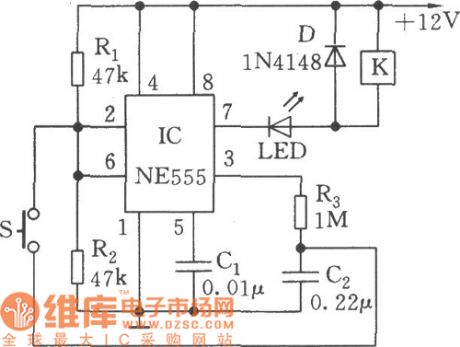
As shown in the figure, 555 is the core of the circuit. Pay attention that R1 = R2 = 47 k Ω and the trigger end feet 2 (set ) connected to 555 and the threshold level end feet 6 (reset); Resistance R3, capacitance C2 for charge and discharge are connected to the output end feet3, and are linked with feet 2 and 6 through the switch. When S disconnects, feet 2, 6 are both 1/2 VDD = 6 V, therefore, the level of feet is random, sometimes it is high, and sometimes it is low. If feet 3 is a high level (about VDD-1. 5 V = 10.5 V), pressing S will add the charge voltage on C2 to feet 6 , to make it higher than trigger level 2/3 VDD, then 555 will be reset, and feet3 will become a low level. (View)
View full Circuit Diagram | Comments | Reading(1337)
Approach Switch Circuit
Published:2011/7/21 1:41:00 Author:Joyce | Keyword: Approach, Switch
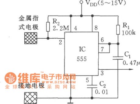
The switch forms a monostable trigger circuit with 555 as the core component .The trigger end feet 2 of is connected with VDD through the major resistance R2, waiting for trigger. When the human body gets close to or touches the metal plate electrode, 555 is activated to output a monostable pulse because of the induction signal. C2 is used to resist interference filter. This circuit can be used for electrical appliances, toys or alarm circuit. (View)
View full Circuit Diagram | Comments | Reading(602)
Remote Multi Point Control Switch Circuit
Published:2011/7/21 18:43:00 Author:Joyce | Keyword: Remote, Multi Point , Control , Switch
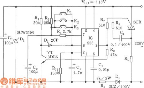
As shown in the figure, the switch circuit includes a depressurization and rectification circuit, a bistable trigger circuit and a silicon controlled control circuit. It will remote control the start up and close down of electric equipment .The depressurization and rectification circuit provides the controller with + 13 V dc voltage. 555, R5, R4, R13, C1, C2, and some other components constitute the bistable trigger circuit. At the moment it is switched on, because the voltage on C1 will not change suddenly, 555 will set, and C2 will be charged to 12V through R5. At this time, if one presses K1 (K2 or Ks), C1 will soon be charged to2/3 VDD = 8 V, and 555 will reset, feet 3 will show a low level, and SCR will cut off. At the same time, VT will cut off; feet 6 of 555 will display a high level to keep 555 in a stable state of reset. (View)
View full Circuit Diagram | Comments | Reading(905)
Inverting_amplifier
Published:2009/7/24 21:32:00 Author:Jessie
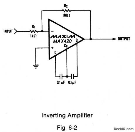
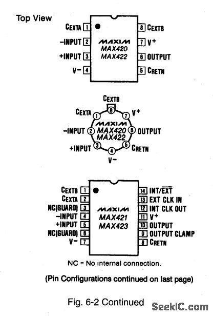
Figure 6-2 shows a chopper-stabilized MAX420 connected as an inverting amplifier. The offset voltage is 5 μV maximum; the input voltage range is + 12 V to -15 V with ±15-V supplies; the input noise is 0.3 μVp-p from dc to 1 Hz; the gain, CMRR, and PSRR are all 120 dB; the maximum supply current is 0.5 mA; and the input bias current is 30 pA. MaxnIM HIGH-RELIABILITY DATA BOOK, 1993, P. 3-11. (View)
View full Circuit Diagram | Comments | Reading(0)
Low_noise_instrumentation_amplifier
Published:2009/7/24 21:30:00 Author:Jessie
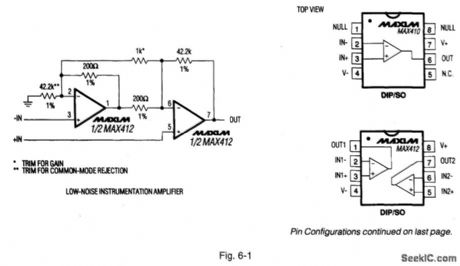

Figure 6-1 shows a low-noise instrumentation amplifier using both sections of a MAX412. Input voltage-noise density is less than 2.4 nV√Hz at 1 kHz. The output voltage swing is 7.3 Vp-p into 2 kΩ from ±5-V supplies. Supply current is 2.5 mA per amplifier, unity-gain bandwidth is 28 MHz, slew rate is 4.5 V/μs, maximum offset voltage is 250 μV, and minimum voltage gain is 115 dB. MAXIM HIGH-RELIABILITY DATA BOOK, 1993, P. 3-9. (View)
View full Circuit Diagram | Comments | Reading(0)
Inductive Automatic Switch Circuit
Published:2011/7/21 18:56:00 Author:Joyce | Keyword: Inductive, Automatic , Switch
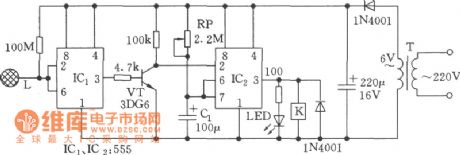
As shown in the figure, two 555s are the core of the automatic switch circuit, IC1 works as a trigger, and IC2 is used as a monostable time circuit. When the human body gets close to or touches the metal plate, IC1 will be triggered to overturn by the induction signal, so feet 3 will display a high level, and VT will be saturated and break over; IC2 will be triggered because feet 2 shows a low level (less than 1/3 VDD), turning into the state of temporary stability. Feet 3 will display a high level, K will actuate and the controlled equipment will be connected. Conversely, it will be disconnected. Timing time is: td = 1.1 RP C1, and it can be regulated by adjusting RP. (View)
View full Circuit Diagram | Comments | Reading(621)
Single_supply_differential_amplifiers
Published:2009/7/24 22:07:00 Author:Jessie
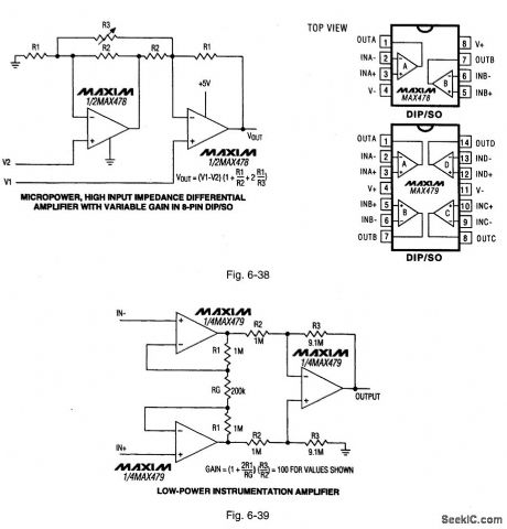
Figure 6-38 shows a MAX478 connected as a differential amplifier with variable gain. Figure 6-39 shows the MAX479 connected as a differential instrumentation amplifier. Both circuits can operate from a single supply, either 3 V or 5 V.Maximum Supply current is 17μA per op amp, the maximum offset voltage is 70 μV, maximum offset-voltage drift is 2.2 μV/℃ (0.5 μV/℃ typical) and maximum input-offset current is 250 pA. MAXIM NEW RELEASES DATA BOOK, 1994, P. 3-59, 3-69. (View)
View full Circuit Diagram | Comments | Reading(985)
Precision_high_gain_differential_amplifier_low_noise
Published:2009/7/24 22:05:00 Author:Jessie

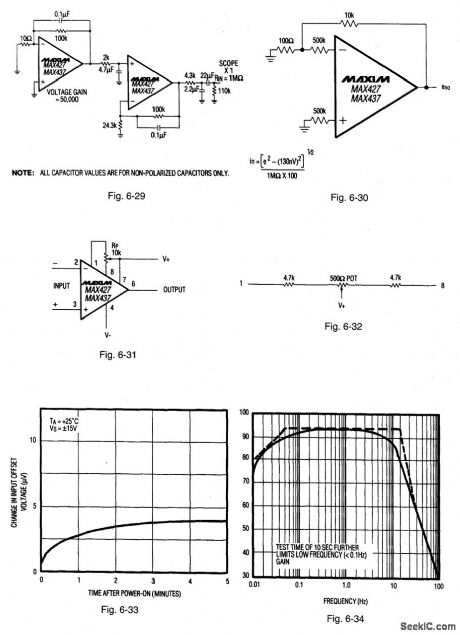
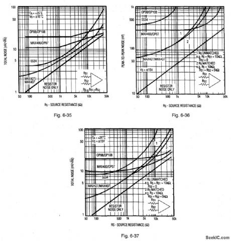
Figure 6-28 shows a MAX427 connected for differential operation. Wideband noise is 2.5 nV√Hz, offset is less than 15 μV (5-μV typical), and drift is less than 0.8 μV/℃ (0.1 μV/℃ typical). The voltage gain is 20 million when driving a 2-kΩ load to±12 V, and 12 million with a 600-Ω load to ±10 V. The MAX427 is unity-gain stable, with an 8-MHz gain-bandwidth, and a 2.5-V/μs slew rate. The decompensated MAX437 has a 60-MHz gain-bandwidth, a 15-V/μs slew rate, and is stable for closed-loop gains of five or greater. Both ICs can be operated from ±5-V supplies. Figures 6-29 and 6-30 show voltage-noise and current-noise test circuits, respectively. Figures 6-31 and 6-32 show offset-voltage adjustment circuits. Figure 6-33 shows typical offset-voltage characteristics. Figures 6-34 through 6-37 show noise characteristics. MAXIM NEW RELEASES DATA BOOK, 1994, P. 3-45. (View)
View full Circuit Diagram | Comments | Reading(1089)
Zero Volt Switch Circuit
Published:2011/7/21 21:21:00 Author:Joyce | Keyword: zero volt , switch
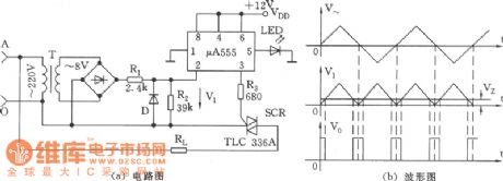
As shown in the figure, the zero volt switch circuit will produce trigger impulse when ac voltage passes zero. In order to achieve it, 555 is connected in the form of a comparator, and corresponding static offset voltage 0.7 ~ 1 V is set on the controlling end feet 5 .A LED is used as comparing device , as well as indication of the existence of the reference voltage . The oscillogram of working process is as shown in figure (b). Here, to illustrate the problem, sine wave is drawn as triangle wave, but analysis of the process will not be influenced.
(View)
View full Circuit Diagram | Comments | Reading(741)
Remotely_powered_sensor_amplifier
Published:2009/7/24 21:56:00 Author:Jessie
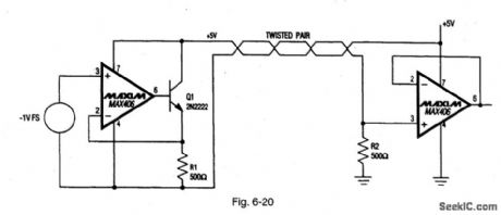
Figure 6-20 shows a simple two-wire current transmitter that uses no power at the transmitting end, except from the transmitted signal itself. At the transmitter, a 0-V to 1-V input drives both a MAX406 and an NPN transistor connected as a voltage-controlled current sink. The 0-mA to 2-mA output is sent through a twisted pair to the receiver and it develops a voltage across receiver sense resistor R2. The resulting sense voltage is buffered by another MAX406, producing a 0-V to 1-V ground-referenced output signal. R1 and R2 should be well matched. The MAX406 supply current is added to the 0-mA to 2-mA signal, resulting in a 500-μV offset at the output. This offset, in addition to the MAX406 input offset, varies with temperature. MAXIM NEW RELEASES DATA BOOK, 1994, P. 3-29. (View)
View full Circuit Diagram | Comments | Reading(0)
Op_amp_bridge_amplifier
Published:2009/7/24 22:50:00 Author:Jessie
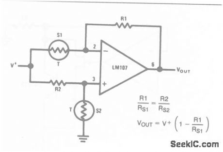
In this circuit, the LM107 serves as the amplifier for two temperature sensors connected In a bridge configuration. As shown by the equations, VOUT depends on the resistance of the sensors. In turn, sensor resistance depends on temperature, so VOUT is related to temperature. See chapter 13 for additional temperature sensing and control circuits. (View)
View full Circuit Diagram | Comments | Reading(719)
RS Trigger Operating Principle Circuit
Published:2011/7/23 1:15:00 Author:Joyce | Keyword: RS , Trigger , Operating Principle
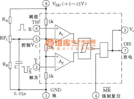
As shown in the figure is a circuit in which 555 works as a RS trigger. If the control voltage on the controlling end feet 5 is removed, there will be no need to connect any external component with 555, but add negative and positive control pulse on feet 2 and 6 respectively to constitute a RS trigger circuit. End R is the reset control input end feet 6, which is also called threshold end (TH);end S is the set control input feet 2, which is also called set trigger end T. The output end (feet 3) within the chip is actually push-pull output, whose low level output is only about 0.3 V and whose high level is close to VDD, so it has a very strong load capacity (View)
View full Circuit Diagram | Comments | Reading(1093)
Schmidt Trigger Circuit and its Trigger Characteristics Circuit
Published:2011/7/21 21:44:00 Author:Joyce | Keyword: Schmidt , Trigger , Characteristics
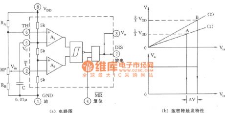
As shown in the figure is a Schmitt trigger composed of time base circuit 555 and a few other components ( RA, RB, RP ). Its threshold voltage is adjustable. It can be seen as being triggered by the comparator. It has two output ends: one is rectangular pulse output by feet 3; the other is discharging waveform (circumscribed capacitor) output by the discharge end (DSC) feet7. (View)
View full Circuit Diagram | Comments | Reading(891)
Changeable Threshold Level Trigger Circuit
Published:2011/7/21 21:54:00 Author:Joyce | Keyword: Changeable , Threshold , Level, Trigger
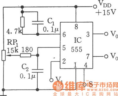
As shown in the figure, with the setting characteristics of reset end feet 4 and trigger end feet 2 of 555, it can compose a RS trigger. Feet 5 is connected with the pressure dividing point 2/3 VDD of the resistance within the substrate. Adding an adjustable control voltage on feet 5 would change the threshold level and trigger level to compose a changeable threshold level Schmidt trigger. C1, C2 are high frequency filter capacitances used to decoupling. (View)
View full Circuit Diagram | Comments | Reading(634)
Biostable Control Circuit
Published:2011/7/21 8:58:00 Author:Joyce | Keyword: Biostable , Control
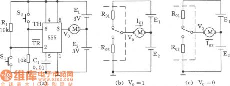
Bistable mode of 555 is applied less commonly compared with monostable mode and nonstable mode. Bistable mode means the circuit it forms will be triggered by pressing R-S. As shown in the figure is micro-motor’s forward/reserve control diagram working under biostable mode. (View)
View full Circuit Diagram | Comments | Reading(574)
| Pages:139/250 At 20121122123124125126127128129130131132133134135136137138139140Under 20 |
Circuit Categories
power supply circuit
Amplifier Circuit
Basic Circuit
LED and Light Circuit
Sensor Circuit
Signal Processing
Electrical Equipment Circuit
Control Circuit
Remote Control Circuit
A/D-D/A Converter Circuit
Audio Circuit
Measuring and Test Circuit
Communication Circuit
Computer-Related Circuit
555 Circuit
Automotive Circuit
Repairing Circuit