
Amplifier Circuit
Index 133
150_MHz_15_W_MOS_amplifier_28_V_supply
Published:2009/7/24 3:36:00 Author:Jessie
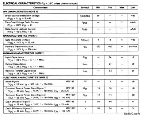
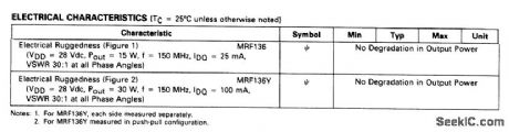
The electrical characteristics for the MRF136 shown in this circuit are given in Fig. 2-48B. (View)
View full Circuit Diagram | Comments | Reading(672)
400_MHz_50_-W_MOS_amplifier28_V_supply
Published:2009/7/24 3:34:00 Author:Jessie
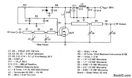
The electrical characteristics for the MRF134 shown in this circuit are given in Fig. 2-46B. Those not familiar with microstrip techniques(for Z1-Z5) should read the many Motorola publications,such as AN548A and AN555. (View)
View full Circuit Diagram | Comments | Reading(978)
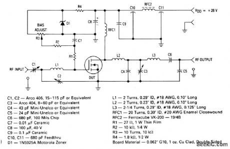
150_MHz_5_W_MOS_amplifier_28_V_supply
Published:2009/7/24 3:32:00 Author:Jessie
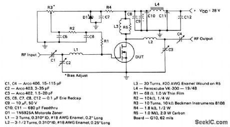
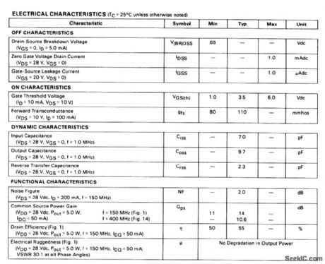
The electrical characteristics for the MRF134 shown in this circuit are given in Fig. 2-46B. (View)
View full Circuit Diagram | Comments | Reading(711)
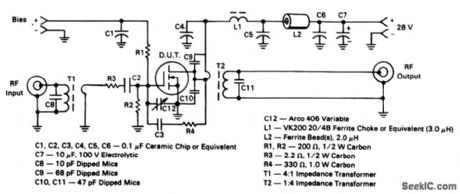
150_MHz_30_W_PEP_MOS_amplifier_28_V_supply
Published:2009/7/24 3:41:00 Author:Jessie
The electrical characteristics for the MRF138 shown in this circuit are given in Fig.2-50B (View)
View full Circuit Diagram | Comments | Reading(625)
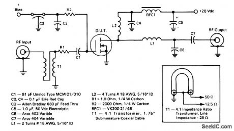
2_to_50_MHZ_30_W_PEP_MOS_amplifier_28_V_supply
Published:2009/7/24 3:39:00 Author:Jessie
The electrical characteristics for the MRF138 shown in this circuit are given in Fig 2-50B (View)
View full Circuit Diagram | Comments | Reading(923)
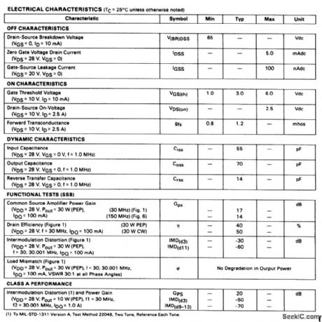
150_MHz_150_W_PEP_MOS_amplifier_28_V_supply
Published:2009/7/24 3:45:00 Author:Jessie
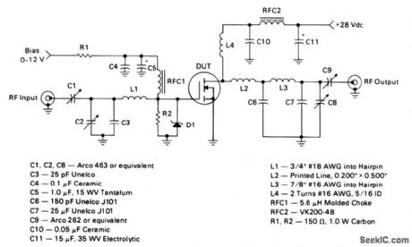
The electrical characteristics for the MRF140 shown in this circuit are given in Fig.2-52B. (View)
View full Circuit Diagram | Comments | Reading(648)
OP_AMP_CLAMPING
Published:2009/7/1 4:49:00 Author:May
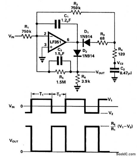
The circuit clamps the most positive value of the input pulse signal to the zero base level. Additionally, the circuit inverts and ampliftes the input signal by the factor of R5/R1. The waveforms are shown in the bottom of Fig. 2-24. (View)
View full Circuit Diagram | Comments | Reading(1212)
HIGH_INPUT_IMPEDANCE_DIFFERENTIAL_AMPLIFIER
Published:2009/7/1 4:29:00 Author:May
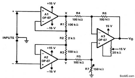
Operational amplifiers A1 and A2 are connected in a non-inverting configuration with their outputs driving amplifier A3. Operational amplifier A3 could be called a subtractor circuit which converts the differential signal floating between points X and Y into a singleended output voltage. Although not mandatonr,_amplifier A3 is usually operated at unity gain and R4, R5, R6, and R7 are all equal.The common-mode-rejection of amplifier A3 is a function of how closely the ratio R4:R5 matches the ratio R6:R7. For example, when using resistors with 0.1% tolerance, common-mode rejection is greater than 60 dB. Additional improvement can be attained by using a potentiometer (slightly higher in value than R6) for R7. The potentiometer can be adjusted for the best common-mode rejection. Input amplifiers Al and A2 will have some differential gain but the common-mode input voltages will experience only unity gain. These voltages will not appear as differential signals at the input of amplifier A3 because, when they appear at equal levels on both ends of resistor R2, they are effectively canceled.This type of low-level differential amplifier finds widespread use in signal processing.It is also useful for dc and low-frequency signals commonly received from a transducer or thermocouple output, which are amplified and transmitted in a single-ended mode.The amplifier is powered by ±15 V supplies. It is only necessary to null the input offset voltage of the output amplifier A3. (View)
View full Circuit Diagram | Comments | Reading(1760)
16__to_30_MHz_100__140__180_W_linear_amplifier_for_mobile_operation
Published:2009/7/24 3:53:00 Author:Jessie
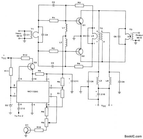
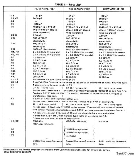
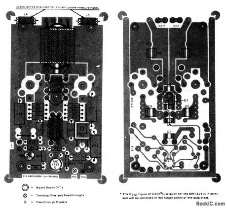
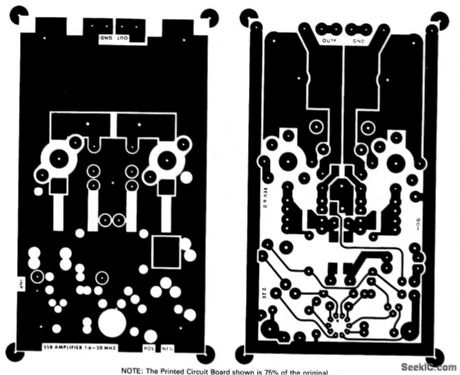
Figure 2-54A shows the basic circuit for the amplifier, and Fig.2-54B shows the parts list for three verslons of the circuit. All three verslons operate with a 13.6-V supply. The component layout,and PC-board layout,are shown in Figs.,2-54C and 2-54D,respectively.Both the parts and kits for this amplifier are available from∶Communications Concepts.121 Brown St, Dayton, Ohio 45402,(513) 220-9677. (View)
View full Circuit Diagram | Comments | Reading(982)
VARIABLE_BOOTSTRAP_FLIP_FLOP_SWEEP
Published:2009/7/24 3:49:00 Author:Jessie
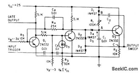
Gives same type of waveform as phontastron. Output pulse length can be varied by d-c bitts or by control voltage.-J. B. Payne III, Voltage-Controlled Bootstrap Generator, Electronics, 33:11, p 177-178. (View)
View full Circuit Diagram | Comments | Reading(822)
SPEECH_COMPRESSOR
Published:2009/7/1 4:20:00 Author:May

The amplifier drives the base of a pnp MPS6517 operating common-emitter with a voltage gain of approximately 20. The control RI varies the quiescent Q point of this transistor so that varying amounts of signal exceed the level Vr. Diode Dl rectifies the positive peaks of Q1's output only when these peaks are greater than Vr ≈ 7.0 volts. The resulting output is filtered Cx, Rx. Rx controls the charging time constant or attack time. Cx is involved in both charge and discharge. R2 (150 K, input resistance of the emitter-follower Q2) controls the decay time. Making the decay long and attack short is accomplished by making Rx small and R2 large, (A Darlington emitter-follower may be needed if extremely slow decay times are required.) The emitter-follower Q2 drives the AGC Pin 2 of the MC1590 and reduces the gain. R3 controls the slope of signal compression. (View)
View full Circuit Diagram | Comments | Reading(1165)
THERMOCOUPLE_AMPLIFIER
Published:2009/7/1 4:15:00 Author:May
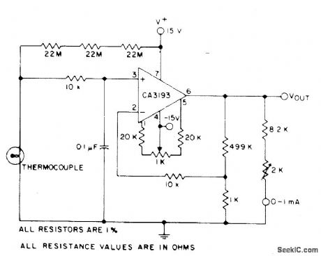
The circuit uses a CA3193 BiMOS precision op amp to amplify the generated signal 500 times. Three 22-megohm resistors will provide full-scale output if the thermocouple opens. (View)
View full Circuit Diagram | Comments | Reading(0)
FLUORESCENT_DISPLAY_DRIVER
Published:2009/7/1 4:15:00 Author:May
National DS8881 vacuum fluorescent display driver handles 16-digit grids. Decode inputs select 1 of 16 outputs to be pulled high. Driver also contains oscillator for supplying clock signals to MOS circuit, filament-bias zener, and 50K pulldown resistors for each grid. Outputs will source up to 7 mA. Supply is 9 V. Interdigh blanking with enable input provides ghost-free display.- In-terface Databook, National Semiconductor, Santa Clara, CA, 1978, p 5-57-5-60.
(View)
View full Circuit Diagram | Comments | Reading(891)
TWO_WIRE_TO_FOUR_WIRE_AUDIO_CONVERTER
Published:2009/7/1 4:15:00 Author:May
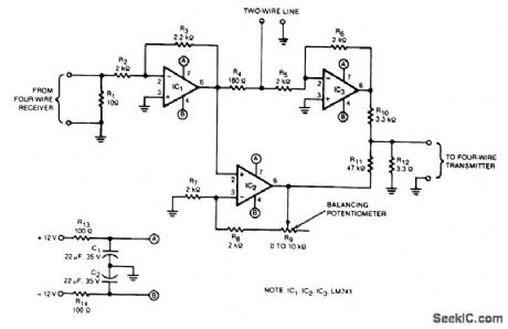
This converter circuit maintains 40 dB of isolation between the input and output halves of a four-wire line while permitting a two-wire line to be connected. A balancing potentiometer, Rg, adjusts the gain of IC2 to null the feed-through from the input to the output. The adjustment is done on the workbench just after assembly by inserting a 1 kHz tone into the four-wire input and setting Rg for minimum output signal. An 82 ohm dummy-load resistor is placed across the two wire terminals. (View)
View full Circuit Diagram | Comments | Reading(729)
Hl_Fl_COMPANDER
Published:2009/7/1 4:13:00 Author:May
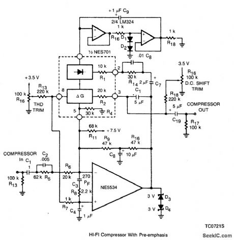
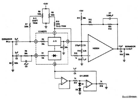
This circuit for a high fidelity compressor uses an external op amp, and has a high gain and wide bandwidth. An input compensation network is required for stability. The rectifier capacitor (C9) is not grounded, but is tied to the output of an op amp circuit. When a compressor is operating at high gain, (small input signal), and is suddenly hit with a signal, it will overload until it can reduce its gain. The time it takes for the compressor to recover from overload is deter-mined by the rectifier capacitor C9. The expandor to complement the compressor is shown in Fig. 2-13B. Here an external op amp is used for high slew rate. Both the compressor and expandor have unity gain levels of 0 dB. Trim networks are shown for distortion (THD) and dc shift. The distortion trim should be done first, with an input of 0 dB at 10 kHz. The dc shift should be adjusted for minimum envelope bounce with tone bursts. (View)
View full Circuit Diagram | Comments | Reading(2536)
CURRENT_COLLECTOR_HEAD_AMPLIFIER
Published:2009/7/1 4:11:00 Author:May
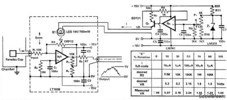
To amplify small current signals such as from an electron,collector inside a vacuum chamber, it is convenient for reasons of noise and bandwidth to have a head-amplifter attached to the chamber. The op-amp N1 is a precision bipolar device with extremely low bias current and offset voltage (1) as well as low noise, which allows the 100:1 feedback attenuator to be employed. The resistance of R3 can be varied from above 10 M to below 1 k, and so the nominal 0 to 1 V-peak output signal corresponds to input current ranges oflnAto10μA. (View)
View full Circuit Diagram | Comments | Reading(0)
LINEAR_AMPLIFIERS_FROM_CMOS_INVERTERS
Published:2009/7/1 4:09:00 Author:May
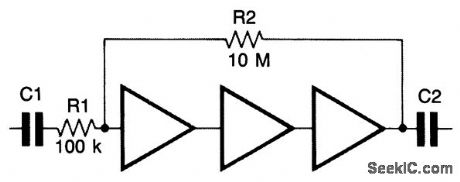
CMOS inverters can be used as linear amplifiers if negative feedback is applied. Best linearity is obtained with feedback applied around three inverters which gives almost perfect linearity up to an output swing of 5 V p-p with a 10 V supply rail. The gain is set by the ratio of R1 and R2 and the values shown are typical for a gain of 100. The high frequency response with the values shown is almost flat to 20 kHz. The frequency response is determined by C1 and C2. This circuit is not suitable for low level signals because the signal-to-noise ratio is only approx. 50 dB with 5 V p-p output with the values shown. (View)
View full Circuit Diagram | Comments | Reading(755)
POWER_GaAsFET_AMPLIFIER_WITH_SINGLE_SUPPLY
Published:2009/7/1 4:08:00 Author:May
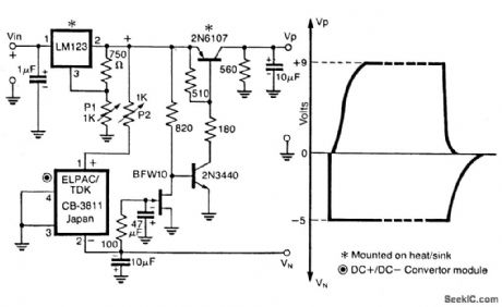
The dual regtilator circuit operates from a positive supply, which when switched ON powers the gate first, and when switched OFF shuts off the drain first as shown in the figure. This circuit incorporates the LM123, a three terminal positive regulator and a dc + to dc - converter, the outputs of which power the drains and gates of the power GaAsFETs in a power amplifier relay. The output of the three terminal regulator drives a dc + to dc - converter whose output biases an N-channel JFET suitably so as to pull the base of the series pass transistor 2N6107 to a level to turn it on. The circuit will turn off the drain supply whenever the negative potential on the Gate fails. (View)
View full Circuit Diagram | Comments | Reading(795)
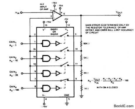
PRECISION_WEIGHTED_RESISTOR_PROGRAMMABLE_GAIN_AMPLIFIER
Published:2009/7/1 4:05:00 Author:May
View full Circuit Diagram | Comments | Reading(927)
STEREO_AMPLIFIER_WITH_GAIN_CONTROL
Published:2009/7/1 4:05:00 Author:May
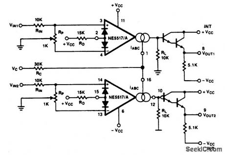
Excellent tracking of typical 0.3 dB is easy to achieve. With the potentiometer, RP, the offset can be adjusted. For ac-coupled amplifiers, the potentiometer may be replacGd with two 5.1 k ohm resistors. (View)
View full Circuit Diagram | Comments | Reading(691)
| Pages:133/250 At 20121122123124125126127128129130131132133134135136137138139140Under 20 |
Circuit Categories
power supply circuit
Amplifier Circuit
Basic Circuit
LED and Light Circuit
Sensor Circuit
Signal Processing
Electrical Equipment Circuit
Control Circuit
Remote Control Circuit
A/D-D/A Converter Circuit
Audio Circuit
Measuring and Test Circuit
Communication Circuit
Computer-Related Circuit
555 Circuit
Automotive Circuit
Repairing Circuit