
Amplifier Circuit
Index 137
MOSFET_INPUT_BUFFER
Published:2009/6/30 1:42:00 Author:May


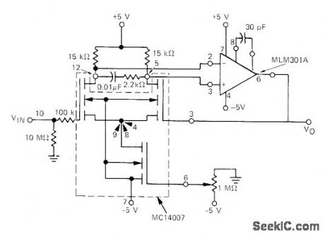
Uses Motorola MC14007 dual complementary pair plus inverter, with two of MOSFETs connected as differential amplifier for buffering opamp and third serving as current source for differential amplifier. Arrangement gives high input impedance required in some applications of MC1505 A/D converter for which buffer was designed. 1-megohm pot controls gate voltage for current source. Temperature drift is well under 2 mV over range of 0-50℃. Pin 14 of MC14007 should be tied to +5 V.—D. Aldridge and S. Kelley, Input Buffer Circuits for the MC1505 Dual Ramp A-to-D Converter Subsystem, Motorola, Phoenix, AZ, 1976, EB-24A. (View)
View full Circuit Diagram | Comments | Reading(2046)
Photodiode_amplifier
Published:2009/7/24 21:00:00 Author:Jessie
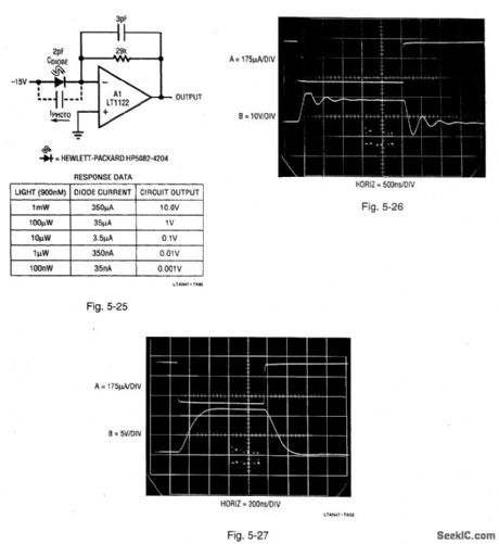
Figure 5-25 shows a basic photodiode amplifier. The table shows various circuit outputs for different diode currents. Figure 5-26 shows circuit response to a photo input (trace A) with the 3-pF feedback capacitor removed. Notice that the output overshoots and saturates before finally ringing down to a level value. Figure 5-27 shows circuit performance with the 3-pF feedback capacitor in place. The same input pulse (trace A, Fig. 5-27) produces a cleanly damped output (trace B).However, the circuit is about 50% faster with the feedback capacitor removed. LINEAR TECHNOLOGY, APPLICATION NOTE 47, P. 41, 42. (View)
View full Circuit Diagram | Comments | Reading(0)
Differential_comparator_amplifier_with_adjustable_limiting_and_offset
Published:2009/7/24 20:59:00 Author:Jessie
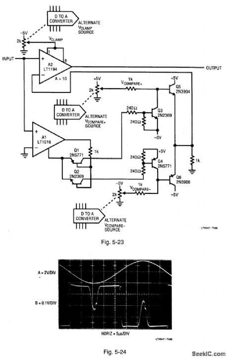
Figure 5-23 is similar to Fig. 5-21, except that the dual channels permit observations of information between two adjustable amplitude-defined points. The set points are adjustable in both magnitude and sign. In the circuit of Fig. 5-23, the polarity of the offset applied to the A2 inverting input is determined by the comparator A1 output state. Figure 5-24 shows the circuit output for a sine input (trace A). The +VCOMPARE and -VCOMPARE voltages are set just below the sine-wave peaks, with VCLAMP set to restrict amplification to the peak excursion. The circuit output (trace B) simultaneously shows the amplitude detail of both sine peaks. LINEAR TECHNOLOGY, APPLICATION NOTE 47, P. 40, 41. (View)
View full Circuit Diagram | Comments | Reading(733)
Fast_differential_comparator_amplifier_with_adjustable_offset
Published:2009/7/24 20:57:00 Author:Jessie

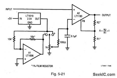
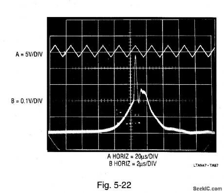
Figure 5-21 shows a circuit that permits one particular portion of a signal to be amplified (or examined) with all other portions rejected. Figure 5-22 shows what happens when the output of a triangle-wave generator (trace A) is applied to the circuit. Setting the bias level just below the triangle peak permits high-gain, detailed observation of the turnaround at the peak. Switching residue in the generator output is observable in trace B. Appropriate variations in voltage-source setting will permit more of the triangle slopes to be observed, (with a loss of resolution because of scope-overload). Similarly, increasing the A2 gain allows more amplitude detail, while placing restrictions on how much of the waveform can be displayed. In effect, this circuit performs the same functions as differential plug-in units for scopes. The circuit output is accurate and settled to 0.1% about 100 ns after entering the linear region. LINEAR TECHNOLOGY, APPLICATION NOTE 47, P. 39, 40. (View)
View full Circuit Diagram | Comments | Reading(760)
Transformer_coupled_amplifier
Published:2009/7/24 20:56:00 Author:Jessie
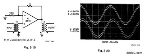
Figure 5-19 shows another way to get high common-mode rejection, together with true 3-port isolation. The input, gain stage, and output are all galvanically isolated from each other. As such, this circuit is useful where large common-mode differences are encountered or where ground integrity is uncertain. With the values shown, A1 has a gain of 11. T1 feeds the A1 input, and the output is taken from T2.Figure 5-20 shows results for a 4-MHz input, with all of the polarity dots referred to ground. The input (trace A, Fig. 5-20) is applied to T1. The output of T1 (trace B) feeds A1. A1 produces gain, and the A1 output (trace C) feeds T2. The T2 output (trace D) is the circuit output. Using the specified transformers, the low-frequency cutoff is about 10 kHz. LINEAR TECHNOLOGY, APPLICATION (View)
View full Circuit Diagram | Comments | Reading(913)
Nonirroerting_amplifier
Published:2009/7/24 20:54:00 Author:Jessie
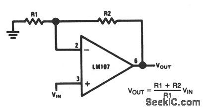
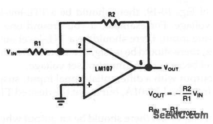
This circuit shows an LM107 in the classic noninverting amplifier configuration, where VOUT follows VIN. The amplitude of the output depends on the ratio of R1 and R2 (within the limits of the supply voltage). The parallel resistance of R1 and R2 should equal the source resistance. (View)
View full Circuit Diagram | Comments | Reading(636)
DAC_amplifier
Published:2009/7/24 20:40:00 Author:Jessie
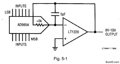
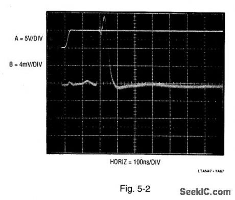
Figure 5-1 shows an amplifier that is suitable for the output of a fast 12-bit DAC (digital-to-analog converter, Chapter 8). Figure 5-2 shows clean 0.01% settling in 280 ns (trace B) to an all-bits-on input step (trace A). LINEAR TECHNOLOGY, APPLICATION NOTE 47, P. 32. (View)
View full Circuit Diagram | Comments | Reading(728)
Inverting_amplifier
Published:2009/7/24 20:53:00 Author:Jessie
This circuit shows an LM107 in the classic inverting-amplifier configuration, where VOUT is opposite to VIN (if VIN goes positive, VOUT goes negative, and vice versa). The amplitude of the output depends on the ratio of R1 and R2 (within the limits of the supply voltage). (View)
View full Circuit Diagram | Comments | Reading(0)
Cable_sense_amplifier_for_loop_through_connections
Published:2009/7/24 20:42:00 Author:Jessie
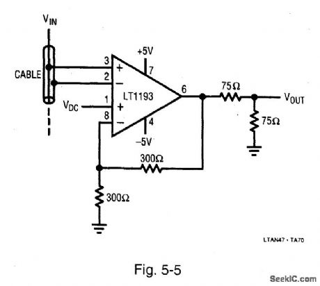
Figure 5-5 shows a differential amplifier used to extract signals from a distribution cable. The amplifier differential inputs reject common-mode signals. Amplifier performance includes 0.02% differential-gain and 0.1° differential-phase errors. A separate input permits dc adjustment. LINEAR TECHNOLOGY, APPLICATION NOTE 47, P. 33. (View)
View full Circuit Diagram | Comments | Reading(640)
Simple_video_amplifier
Published:2009/7/24 20:41:00 Author:Jessie
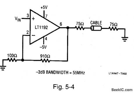
Figure 5-4 is a simpler version of Fig. 5-3, but with only one video channel. The bandwidth of 55 MHz. LINEAR values provide for a gain of 10, with a TECHNOLOGY, APPLICATION NOTE 47, P. 33. (View)
View full Circuit Diagram | Comments | Reading(0)
Two_channel_video_amplifier
Published:2009/7/24 20:41:00 Author:Jessie
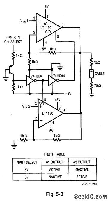
Figure 5-3 shows a simple way to multiplex two video amplifiers onto a single 75-Ω cable. The appropriate amplifier is activated in accordance with the truth table. Amplifier performance includes 0.02% differential-gain and 0.1°differential-phase errors. The 75-Ω back termination looking into the cable means that the amplitude must swing 2 Vp-p to produce 1-Vp-p at the cable output. LINEAR TECHNOLOGY, APPLICATION NOTE 47, P. 33. (View)
View full Circuit Diagram | Comments | Reading(763)
FET_INPUT_BUFFER
Published:2009/6/30 1:31:00 Author:May
Used ahead of Motorola MC1505 A/D converter to provide input impedance of 10 megohms. FETs are connected as differential amplifier having common source leads returned to constant-current generator built from bipolar transistor, with similar transistor providing temperature compensation. Temperature drift of amplifier is well under 1 mV from 0 to 50℃.—D. Aldridge and S. Kelley, Input Buffer Circuits for the MC1505 Dual Ramp A-to-D Converter Subsystem, Motorola, Phoenix, AZ, 1976, EB-24A. (View)
View full Circuit Diagram | Comments | Reading(1001)
DIFFERENTIAL_OPAMP_AS_BUFFER
Published:2009/6/30 1:30:00 Author:May

Section of Motorola MC3403 quad opamp, operating from single supply, serves as low-cost unity-gain buffer for MC1505 dual-ramp A/D converter. Opamp is used as differential amplifier referenced to MC1505 reference voltage of 1.25 V,—D. Aldridge and S. Kelley, Input Buffer Circuits for the MC1505 Dual Ramp A-to-D Converter Subsystem, Motorola, Phoenix, AZ, 1976, EB-24A. (View)
View full Circuit Diagram | Comments | Reading(990)
HIGH_IMPEDANCE_BUFFER
Published:2009/6/30 1:26:00 Author:May
Two sections of Motorola MC3403 quad opamp serve as voltage followers for differential inputs of third section connected as buffer for MC1505 A/D converter.Dual transistor 01, connected as dual diode, provides 0.6-V offset at inputs of voltage followers, to obtain temperature tracking and predictable performance at low bias currents of opamp.—D. Aldridge and S. Kelley, Input Buffer Circuits for the MC1505 Dual Ramp A-to-D Converter Subsystem, Motorola, Phoenix, AZ, 1976, EB-24A. (View)
View full Circuit Diagram | Comments | Reading(1164)
COMPRESSOR_1
Published:2009/6/29 23:59:00 Author:May
Keeps output voltage constant as long as input signal is kept above AP threshold level. Opamp is MC3340P. -Circuits, 73 Magazine, Holiday issue 1976, p 170. (View)
View full Circuit Diagram | Comments | Reading(918)
VOX_WITH_SPEECH_COMPRESSION
Published:2009/6/29 23:58:00 Author:May
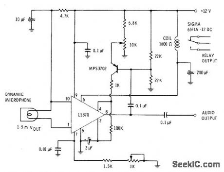
Turns on transmitter automatically when operator begins speaking into microphone. Circuit switches back to receiving condition automatically at end of message. IC can be LS370 or equivalent such as LM370 or SC370. Amount of compression is adjusted with 10K pot, for reducing gain of IC automatically to maintain reasonably constant audio output at pin 8 despite different voice levels at microphone.-E. M.Noll, Linear 10 Principles, Experiments, and Projects, Howard W.Sams,Indianapolis, IN, 1974, p 344-347. (View)
View full Circuit Diagram | Comments | Reading(2549)
8_BIT_SUCCESSlVE_APPROXlMATION
Published:2009/6/29 23:57:00 Author:May
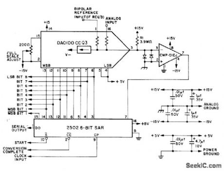
Uses Precision Monolithics DAC-100 CCO3 D/A converter and CMP-01CJ fast precision comparator in combination with Advanced Micro Devices AM2502PC or equivalent successive approximation register to compare analog input with series of trial conversions. Clamp diodes minimize settling time and prevent large inputs from damaging DAC output. Digital output is available in serial nonreturn-to-zero format at data output DO shortly after each positivegoing clock transition.—D. Soderquist, A Low Cost, Easy-to-Build Successive Approximation Analog-to-Digital Converter, Precision Monolithics, Santa Clara, CA, 1976, AN-11, p 3. (View)
View full Circuit Diagram | Comments | Reading(778)
Amplifier circuit of RF2131 with best power and efficiency at 4.0~4.8V power supply
Published:2011/5/6 1:43:00 Author:May | Keyword: Amplifier, 4.0~4.8V power supply, best power and efficiency
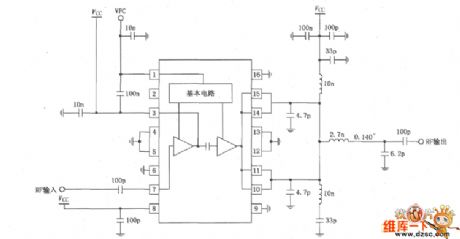
Amplifier circuit of RF2131's best power and efficiency at 4.0~4.8V power supply is shown in the diagram:
(View)
View full Circuit Diagram | Comments | Reading(632)
COMPRESSOR
Published:2009/6/29 23:49:00 Author:May
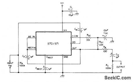
Circuit has unity gain at 0.775 VRMS input and complementary input/output characteristic. Voltage gain through compres sor is square root of 0.7/VIN where VIN is avefage input voltage. Uses Signetics dualchannel compandor IC; 571 has lower inherent distortion and higher supply voltage range (6-24 V) than 571 (6-18 V).-W. G. Jung, Gain Control IC for Audio Signal Processing, Ham Radio, July 1977, p 47-53. (View)
View full Circuit Diagram | Comments | Reading(5482)
Increasing_amplifier_output_current_and_voltage_swing
Published:2009/7/24 23:23:00 Author:Jessie
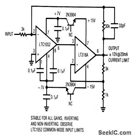
This circuit increases both the output current and the voltage-swing capability for a typical IC amplifier. The transistors run in the Zener mode, dropping the supply to about±7 V at the LTC1052. The LT318A serves as an output stage with a voltage gain of 4. The output swing is typically±13 V into 2 kΩ, with a short-circuit current of 20 mA. The circuit is dynamically stable at any gain, either inverting or noninverting. However, the LTC1052 input common-mode range (-7 V to +5 V with the ±15-V supply) must not be exceeded. (View)
View full Circuit Diagram | Comments | Reading(902)
| Pages:137/250 At 20121122123124125126127128129130131132133134135136137138139140Under 20 |
Circuit Categories
power supply circuit
Amplifier Circuit
Basic Circuit
LED and Light Circuit
Sensor Circuit
Signal Processing
Electrical Equipment Circuit
Control Circuit
Remote Control Circuit
A/D-D/A Converter Circuit
Audio Circuit
Measuring and Test Circuit
Communication Circuit
Computer-Related Circuit
555 Circuit
Automotive Circuit
Repairing Circuit