
Amplifier Circuit
Index 138
Increasing_amplifier_output_current
Published:2009/7/24 23:22:00 Author:Jessie
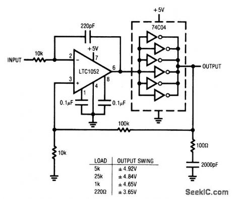
his circuit parallels a package of CMOS inverters to obtain 10- to 20-mA output current capability for a typical IC amplifier (such as an op amp). The values shown for the inversion feedback loop (10 kΩ/100 kΩ) and the RC damper (100Ω/2000 pF) are for the ICs shown. These values can be changed to accommodate other IC amplifiers. (View)
View full Circuit Diagram | Comments | Reading(820)
Digitally_controlled_variable_gain_amplifier
Published:2009/7/24 23:21:00 Author:Jessie
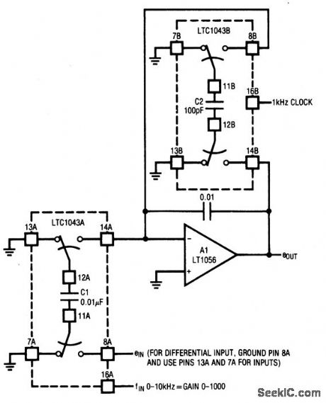
This circuit provides a continuously-variable gain from 0 to 1000, with a stability of 20 ppm/℃. Either a single-ended or differential input can be selected.A host processor selects the desired gain by applying the corresponding frequency at pin 16A of the LTC1043A. The LTC1043B is continuously clocked by a 1-kHz source (which can also be supplied by the host processor). For the values given, gain is: (fIN×10) × (0.01 μF/100 pF). Gain stability depends on the ratiometric stability between the 1-kHz clock and the variable clock (pin 16A). For this reason, both the fixed and variable clocks should be supplied by the same source (probably a processor). (View)
View full Circuit Diagram | Comments | Reading(900)
High_speed_low_noise_instrumentation_amplifier
Published:2009/7/24 21:47:00 Author:Jessie

Figure 6-12 is similar to Fig. 6-1, except for the op-amp characteristics. For the LT1028, the input voltage-noise density is 1.1 nV√Hz maximum at 1 kHz, 0.85 nV√Hz typical at 1 kHz, 1.0 nV√Hz typical at 10 Hz, and 35 nVp-p typical at 0.1 Hz to 10 Hz. Minimum gain-bandwidth is 50 MHz, minimum slew rate is 10 V/μs, maximum offset voltage is 40 μV, and maximum offset drift is 0.8 μV/℃. Minimum voltage gain is 7 million. MAXIM NEW RELEASES DATA BOOK, 1993, P. 3-59. (View)
View full Circuit Diagram | Comments | Reading(918)
COMPANDER_WITH_100dB_RANGE
Published:2009/6/29 22:46:00 Author:May
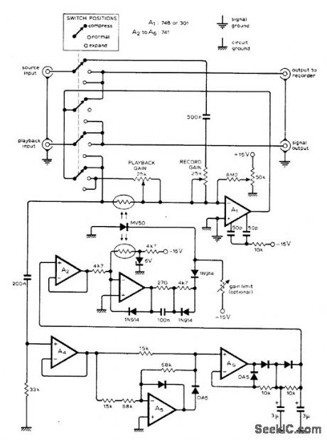
Simple squarelaw circuit preserves dynamic range of virtually any input signal when recorded by or dinary tape recorder. Suitable for speech signals as well as for recording or playback in noisy environments. Opamp A1 should have separately decoupled supply. Switching provides compression during recording and expansion during playback. Tracking of photocells is essential for accurate power-law compansion, LED can be glued with clear epoxy to matched photocells. Use silicon signal diodes such as 1N914, 1N4148, or 1S44. Inexpensive photocells such as Vactec VT-833 gave suitably low distortion. Article gives performance characteris-tics and operating details.-J. Vanderkooy, Wideband Compander Design, Wireless World, July 1976, p 45-49. (View)
View full Circuit Diagram | Comments | Reading(1274)
PREEMPHASIS_AT_1500_Hz
Published:2009/6/29 22:31:00 Author:May
Single-transistor peaking filter is combined with low-noise RFprotected preamp stage to improve speech intelligibility for any type of modulation. Effectiveness is most noticeable with deep bass voice, where soft peak around 1500-2000 Hz improves speech intelligibility. Can also serve as audio-type CW or SSB filter-You Can Sound Better with Speech Pre-Emphasis, 73 Magazine, Feb. 1977, p 42-43. (View)
View full Circuit Diagram | Comments | Reading(1464)
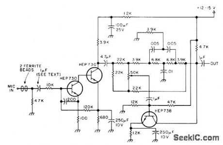
HI_FI_COMPRESSOR
Published:2009/6/29 22:28:00 Author:May
One section of Signetics NE570 dual compandor is used with extemal opamp for compression of large input signals in high-fidelity audio system. To prevent overload by sudden loud signal when compressor is operating at high gain for small signals, bruteforce clamp diodes D3 and D4 limit output swings to about 7V P-P, Limiting action prevents overloading of succeeding circuit such as tape recorder. Circuit includes input compensation network required for stability. Corresponding expander used for playback of recorded material should have same value for rectifier capacitor C9 as is used in compressor.- SignetIcs Analog Data Manual, SignetIcs, Sunnyvale, CA, 1977, p 804. (View)
View full Circuit Diagram | Comments | Reading(2337)
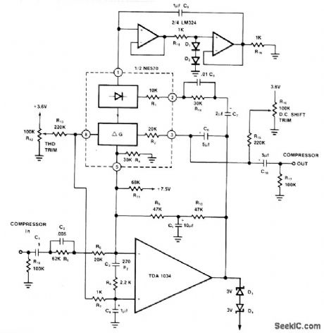
INVERTING_AC_AMPLIFIER
Published:2009/6/29 22:21:00 Author:May
Provides gain of 40 dB when using 24-V supply and input impedance greater than 10K. Low-frequency performance is flat to 20 Hz. Design procedure is given.- Audio Handbook, National Semiconductor, Santa Clara, CA,1977, p 2-20-2-24. (View)
View full Circuit Diagram | Comments | Reading(876)
BALANCED_INPUT_MICROPHONE_PREAMP
Published:2009/6/29 22:21:00 Author:May
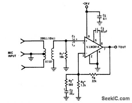
Use of two wires for microphone signal and separate wire for ground keeps hum and noise at minimum. Signal wires are twisted together in shield acting as ground. Net gain is 52 dB, giving 0-dBm output for nominal 2-mV input.Noise performance is -86 dB below 2-mV input level, and rejection of commonmode signals is 60 dB.- Audio Handbook, National Semiconductor, Santa Clara, CA, 1977, p 2-37-2-40. (View)
View full Circuit Diagram | Comments | Reading(897)
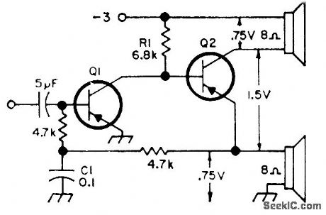
BRIDGE_AMPLIFIER_1
Published:2009/6/29 22:17:00 Author:May
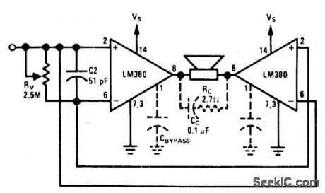
Two opamps are used in bridge configuration to provida twice the voilage swing across loudspeaker load for given 18-V supply,increasing power capability to about twice that of single amplifier.To eliminate excessive quiescent DC voltage across load,nonpolarized capacitor can be used in series with load or 1-megohm pot can be connected between pins 1 of opampswith position of moving arm adiusted to balance offset voltage Components shown with dashed Iines are added for stability with high-current load.-"Audio Handbook, National Semiconductor,Santa Clara, CA.1977,p 4-21-4-28. (View)
View full Circuit Diagram | Comments | Reading(876)
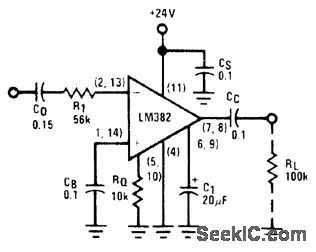
ULTRALOW_NOISE_PREAMP
Published:2009/6/29 22:16:00 Author:May
Provides gain of 1000 over bandwidth of 20 Hz to 10 kHz, operating from 24-V supply and 600-ohm source impedance. Design procedure is given. Total wideband noise voltage is 43.7μA, and wideband noise figure is 2.83 dB.- Audio Handbook, National Semiconductor, Santa Clara, CA, 1977, p 2-15-2-19. (View)
View full Circuit Diagram | Comments | Reading(1105)
IMPEDANCE_BUFFER
Published:2009/6/29 22:15:00 Author:May
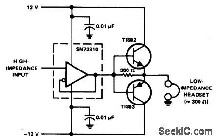
Complementary-transistor output stage provides required low impedance for driving headphones from SN72310 voltage-follower opamp. Supply is ±12V.- The Linear and Interface Circuits Data Book for Design Engineers, Texas Instruments,Dallas,TX,1973,p 4-41 (View)
View full Circuit Diagram | Comments | Reading(928)
PREAMP_IN_MIKE
Published:2009/6/29 22:10:00 Author:May
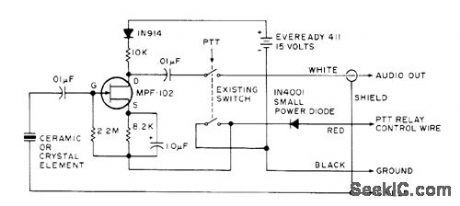
Common-source FET preamp and 15-V battery fit into Turner 3500 hand mike for boosting output of ceramic element 20 dB. Frequency response of preamp is flatfrom 200 Hz to over 100 kHz,Drain is 200 μA only when push-to-talk is pressed、giving long battery life.-G. Hinkle、 Self-Powered Mike Preamp,73 Magazine, Nov.1976,p 65 (View)
View full Circuit Diagram | Comments | Reading(983)
50_mW_FLAT_TO_30_kHz
Published:2009/6/29 22:09:00 Author:May
Power amplifier achieves push-pull output with single transistor. Both transistors should be germanium such as 2N404 SK3004 or HEP-253.-Circuits, 73 Magazine, Feb. 1974, p 100. (View)
View full Circuit Diagram | Comments | Reading(2128)
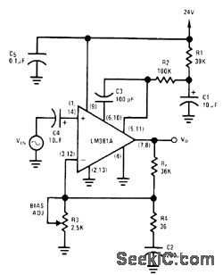
Offset voltage adjustment voltage follower circuit
Published:2011/7/28 20:50:00 Author:John | Keyword: Offset voltage adjustment, voltage follower
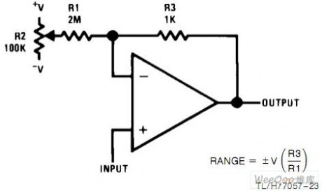
Offset voltage adjustment voltage follower circuit is shown.
(View)
View full Circuit Diagram | Comments | Reading(2883)
LOW_NOISE_OPAMP_PREAMP
Published:2009/6/29 22:07:00 Author:May
Circuit combines noise features of discrete design with simplicity and high open-loop of IC opamp such as 741. Transistors can be 2N3708, BC109, or equivalent. Output impedance is low enough to drive headphones directly.-D. R. Hedgeland, 0p-Amp Pre-Amp, Wireless World, Dec, 1972, p 575. (View)
View full Circuit Diagram | Comments | Reading(1511)
Fast_integrator
Published:2009/7/24 21:20:00 Author:Jessie
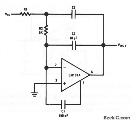
This circuit improved by about is similar to that of Fig. 10-10, except that settling time is 10 to 1. (View)
View full Circuit Diagram | Comments | Reading(1430)
Integrator
Published:2009/7/24 21:18:00 Author:Jessie
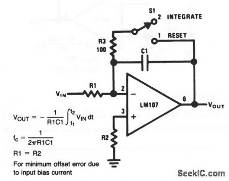
This circuit was originally developed to perform the mathematical operation of integration in analog computers. An integrator is essentially a low-pass filter with a frequency response that decreases at 6 dB per octave. When S1 is in position 1, C1 is discharged, which sets an initial condition of 0 V. With S1 in position 2, the amplifier is connected as an integrator, where the output changes in accordance with a constant times the time-integral of the input. (View)
View full Circuit Diagram | Comments | Reading(1)
Differentiator
Published:2009/7/24 21:17:00 Author:Jessie
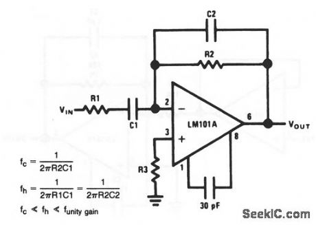
This circuit was originally developed to perform the mathematical operation of differentiation in analog computers. R2C2 form a 6-dB per octave rolloff network in the feedback, and R1/C1 for a similar network at the input making a differentiator a form of filter. The frequency fc refers to the relative frequency at unity gain, while fh refers to the frequency with a voltage gain of 20 dB. (View)
View full Circuit Diagram | Comments | Reading(0)
Noniverting_ac_amplifier
Published:2009/7/24 21:14:00 Author:Jessie
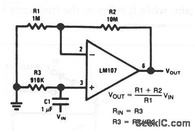
This circuit is similar to that of Fig. 10-2, except that C1 blocks dc inputs, but passes ac inputs. (View)
View full Circuit Diagram | Comments | Reading(658)
Fast_inverting_amplifier_with_high_input_impedance
Published:2009/7/24 21:14:00 Author:Jessie
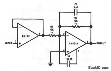
This circuit is similar to that of Fig. 10-6, except that settling time is improved by about 10 to 1. (View)
View full Circuit Diagram | Comments | Reading(0)
| Pages:138/250 At 20121122123124125126127128129130131132133134135136137138139140Under 20 |
Circuit Categories
power supply circuit
Amplifier Circuit
Basic Circuit
LED and Light Circuit
Sensor Circuit
Signal Processing
Electrical Equipment Circuit
Control Circuit
Remote Control Circuit
A/D-D/A Converter Circuit
Audio Circuit
Measuring and Test Circuit
Communication Circuit
Computer-Related Circuit
555 Circuit
Automotive Circuit
Repairing Circuit