
Amplifier Circuit
Index 123
80_W_PEP_broadband_linear_amplifier
Published:2009/7/23 22:56:00 Author:Jessie
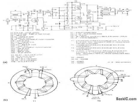
This circuit provides 80-W (PEP)into a 50-Ω load.Figure 2-51B shows the transformer details. (View)
View full Circuit Diagram | Comments | Reading(708)
PRF_MULTIPLIER
Published:2009/7/23 22:55:00 Author:Jessie
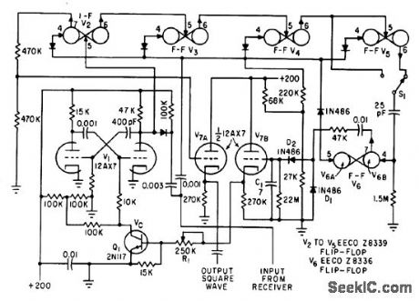
Multiplies pulse repetition frequency of ultrasonic receiver by factor of either 4 or 8, into range between 35 and 85 cps at which synchronous motors of indicalor system work best, Multiplication is based on controlled mvbr oscillator V1, whose frequency can be varied from 40 to 180 cps by varying control voltage Vc. Multiplier feedback circuit acts to control this voltage so mvbr frequency is exact multiple, 8 or 16, of input pulse rate.-H. F. Messias, Ultrasonics Measures Flow Velocity of Rivers, Electronics, 34:41, p 56-69. (View)
View full Circuit Diagram | Comments | Reading(658)
Photovoltaic_cell_amplifier
Published:2009/7/23 22:18:00 Author:Jessie
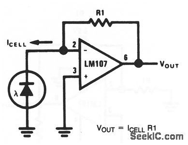
As shown by the equation, VOUT depends on photovolataic-cell current and R1 (which should be chose for or scale factor) (View)
View full Circuit Diagram | Comments | Reading(925)
Simple_SSB_IF_amplifier
Published:2009/7/23 22:17:00 Author:Jessie
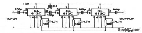
This circuit uses three SL612C amplifiers, and provides a gain of 100 dB at 9 MHz. (View)
View full Circuit Diagram | Comments | Reading(628)
Williams tube amplifier circuit diagram
Published:2011/8/1 22:32:00 Author:Ecco | Keyword: Williams , tube amplifier
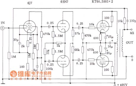
View full Circuit Diagram | Comments | Reading(1175)
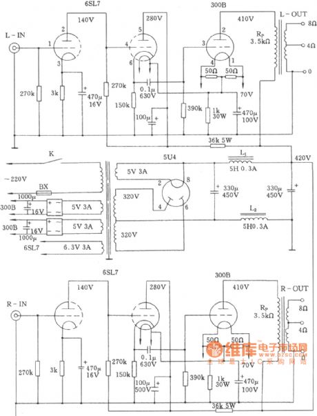
Dynaco ST70 tube amp circuit diagram
Published:2011/8/1 22:34:00 Author:Ecco | Keyword: Dynaco, tube amp
View full Circuit Diagram | Comments | Reading(2821)
300b tube power amp circuit diagram
Published:2011/8/1 22:43:00 Author:Ecco | Keyword: tube power amp
View full Circuit Diagram | Comments | Reading(4444)
225_MHz_13_W_AMPLIFIER_
Published:2009/7/4 20:45:00 Author:May
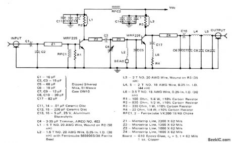

Suitable for use in FM transmitters for 220-225 MHz amateur radio bandBandwidth is about 10 MHz for ±0.5 dB Low-pass filter provides about 60-dB attenuation of second harmonic. Microstrip matching network simplifies construction. Supply 13-Watt Microstdp Amplifier for 220-225 MHz FM tranBandwidth is about 10 MHz for t0.5smitters for 220-225 MHz amateur ing network simplifies construction. Supply voltage is 12.5 V.-J. Hatchett and T. Sallet ''13-Watt Microstdp Amplifier for 220-225 MHz Operation, , Motorola, Phoenix, AZ, 1975, AN728, p 3. (View)
View full Circuit Diagram | Comments | Reading(756)
VHF_POWER_AMPLIFIER
Published:2009/7/4 20:24:00 Author:May
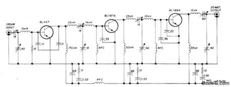
Three-stage 25-W225-MHz power amplifier module for FM apρlications uses three Amperex power transistors,Input and output are 50 ohms With 100-mW input signal,output is 25 W. Four capacitive dividers serve for input, output, and interstage matching. Collectors are shunt-fed. Three decoupling networks prevent seff-oscillation. Ampilfer can withstand output mismatches as high as 50:1 without damage.-E. Noll, VHF/ UHF Single-Frequency Conversion, Ham Radio, April 1975, p 62-67. (View)
View full Circuit Diagram | Comments | Reading(962)
AFC_AMPLIFIER_
Published:2009/7/4 20:03:00 Author:May
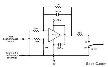
Simple DC amplifier can be added to AFC circuit of FM tuner to eliminate tuning errors over entire lock-in range.-J. S.Wilson, Improved A.F.C. for F.M. Tuners, Wireless World, July 1974, p 239. (View)
View full Circuit Diagram | Comments | Reading(1311)
1_GHz_amplifier_mixer
Published:2009/7/23 22:21:00 Author:Jessie
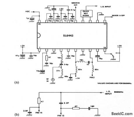
This circuit shows an SL6442 used as an amplifier/mixer suitable for cordless or cellular telephones, pagers, and any low-power receiver operating at frequencies up to 1GHz. The SL6442 contains a low-noise amplifier with AGC and two mixers for use in I and Q direct-conversion receivers or image-canceling in superhet receivers, with a single 5-V supply at a typical current of 4 mA. In this circuit, the local-oscillator signal is applied through a quad network (Fig. 2-33B).RF is applied at pin 4, AGC at pin 20, and mixer outputs are taken from pins 11 and 15. (View)
View full Circuit Diagram | Comments | Reading(1060)
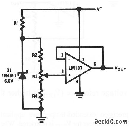
Positive_variable_voltage_reference_vout_is_higher_than_reference_zener
Published:2009/7/23 22:19:00 Author:Jessie
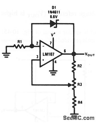
High-preclsion extended-temperature applications of this circult require that the range of adjustment for VOUT is restricted,When this is done,R1 can be chosen to provide optimum zener current for minimum zener temrerature coefficient (TC). Because zener current IZ is not a function of V+,reference TC is independent of V+.
(View)
View full Circuit Diagram | Comments | Reading(706)
VOLTAGE_FOLLOWER_AMPLIFIER_FOR_SIGNAL_SUPPLY_OPERATION
Published:2009/7/3 5:25:00 Author:May
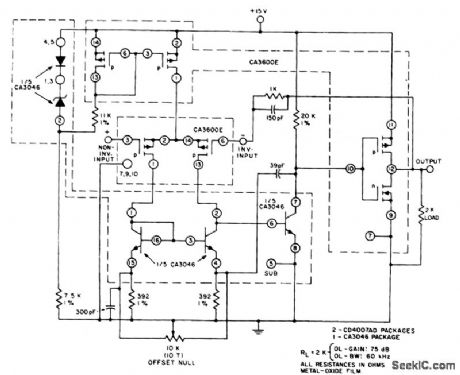
This unity-gain follower amplifier has a CMOS p-channel input, an npn second-gain stage, and a CMOS inverter output. The IC building blocks are two CA3600E's (CMOS transistor pairs) and a CA3046 npn transistor array. A zener-regulated leg provides bias for a 400-μA p-channel source, feeding the input stage, which is terminated in an npn current mirror. The amplifier voltage-offset is nulled with the 10-KΩ balance potentiometer. The second-stage current level is established by the 20-KΩ load, and is selected to approximately the first-stage current level, to assure similar positive and negative slew rates. The CMOS inverter portion forms the final output stage and is terminated in a 2-KΩ load, a typical value used with monolithic op amps. Voltage gain is affected by the choice of load resistance value. The output stage of this amplifier is easily driven to within 1 mV of the negative supply voltage. (View)
View full Circuit Diagram | Comments | Reading(1487)
LOW_NOISE_PHOTODIODE_AMPLIFIER
Published:2009/7/3 5:23:00 Author:May
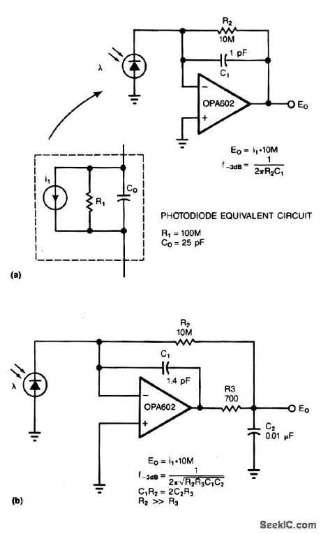
Adding two passive components to a standard photodiode amplifier reduces noise. Without the modifi-cation, the shunt capacitance of the photodiode reacting with the relatively large feedback resistor of the transimpedance (current-to-voltage) amplifier, creates excessive noise gain.
The improved circuit, Fig. 3-18b, adds a second pole, formed by R3 and C2. The modifications reduce noise by a factor of 3. Because the pole is within the feedback loop, the amplifier maintains its low output impedance. If you place the pole outside the feedback loop, you have to add an additional buffer, which would increase noise and dc error.
The signal bandwidth of both circuits is 16 kHz. In the standard circuit (Fig. 3-18a), the 1-pF stray capacitance in the feedback loop forms a single 16-kHz pole. The improved circuit has the same bandwidth as the first, but exhibits a 2-pole response. (View)
View full Circuit Diagram | Comments | Reading(2170)
WRITE_AMPLIFIER
Published:2009/7/3 5:21:00 Author:May
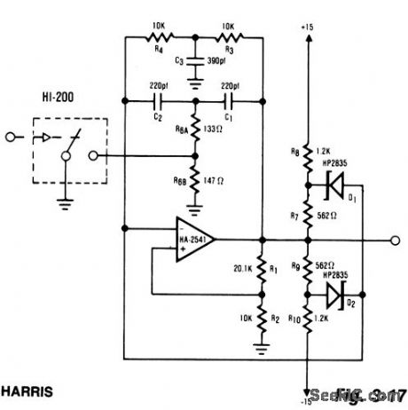
The proliferation of industrial and computerized equipment containing programmable memory has increased the need for reliable recording media.The magnetic tape medium is presently one of the most widely used methods. The primary component of any magnetic recording mechanism is the write mechanism. The concept of the write generator is very basic. The digital input causes both a change in the output amplitude, as well as a change in frequency. This type of operation is accomplished by altering the value of a resistor in the standard twin-tee oscillator. A HI-201 analog switch was used to facilitate the switching action. The effect of the external components on the feedback network requires R6A and R6B to be much smaller than would normally have been expected when using the twin-tee feedback scheme. (View)
View full Circuit Diagram | Comments | Reading(805)
Positive_variable_voltage_reference_VSUBOUT_SUB_is_lower_than_reference_zener
Published:2009/7/23 22:23:00 Author:Jessie
This circuit is suited for high-precision extended-temperature service, if V+ is reasonably constant (Because IZ does depend on V+). R1 through R4 are chosen to provide optimum zener current for minimum zener temperature coeffi-cient (TC), and to minimize error of Ibis. (View)
View full Circuit Diagram | Comments | Reading(660)
UNITY_GAIN_VIDEO_SAMPLING_AMPLIFIER
Published:2009/7/23 22:22:00 Author:Jessie
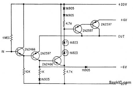
Five-transistor amplifier delivers high bidirectional current, with bandwidth of 10 Mc, for amplifying incoming radar or other pulse prior to binary conversion.-A. Hakimoglu and R. D. Kulvin, Sampling Ten Million Words a Second, Electronics, 37:6, p 52-57. (View)
View full Circuit Diagram | Comments | Reading(667)
DC_STBILIZED_FAST_AMPLIFIER
Published:2009/7/3 5:20:00 Author:May
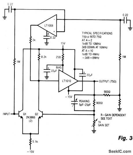
This amplifier functions over a wide range of gains, typically 1 -10. It combines the LT1010 and a fast discrete stage with an LT1008 based dc stabilizing loop. Q1 and Q2 form a differential stage which single-ends into the LT1010. The circuit delivers 1 V pk-pk into a typical 75-Ω video load. At A = 2, the gain is within 0.5 dB to 10 MHz with the -3-dB point occurring at 16 MHz. At A = 10, the gain is flat (± 0.5 dB to 4 MHz) with a -3-dB point at 8 MHz. The peaking adjustment should be optimized under loaded output conditions. This is a simple stage for fast applications where relatively low output swing is required. Its 1 V pk-pk output works nicely for video circuits. A possible problem is the relatively high bias current, typically 10 μA. Additional swing is possible, but more circuitry is needed. (View)
View full Circuit Diagram | Comments | Reading(678)
AC_COUPLED_DYNAMIC_AMPLIFIER
Published:2009/7/3 5:07:00 Author:May

This circuit acts as a bandpass filter with gain and would be most useful for biomedical instrumen-tation. Low-frequency cutoff is set at 10 Hz while the high-frequency breakpoint is given by the openloop rolloff characteristic of the HA-5141/42/44. In this case, the AVCL= 60 dB where the rolloff occurs at approximately 300 Hz. This comer frequency may be trimmed by inserting a capacitor in parallel with Rf. (View)
View full Circuit Diagram | Comments | Reading(793)
Low_drift_integrator
Published:2009/7/23 22:36:00 Author:Jessie
Compare this circuit to that of Fig. 10-41. Hero, the mechanical switch is replaced by Q1 and Q2. (View)
View full Circuit Diagram | Comments | Reading(635)
| Pages:123/250 At 20121122123124125126127128129130131132133134135136137138139140Under 20 |
Circuit Categories
power supply circuit
Amplifier Circuit
Basic Circuit
LED and Light Circuit
Sensor Circuit
Signal Processing
Electrical Equipment Circuit
Control Circuit
Remote Control Circuit
A/D-D/A Converter Circuit
Audio Circuit
Measuring and Test Circuit
Communication Circuit
Computer-Related Circuit
555 Circuit
Automotive Circuit
Repairing Circuit