
Amplifier Circuit
Index 135
High_precision_weight_scale
Published:2009/7/24 5:11:00 Author:Jessie
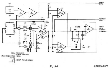
Figure 4-7 shows a switched-capacitor type of bridge circuit used in weight-scale applications. (The circuit is intended for weighing human subjects.) Resolution is 0.01 pound at 300.00 pounds, full scale. To trim the circuit, adjust the zero pot for 0 V out with no weight on the platform. Then set the gain adjustment for 3.0000-V output for a 300.00-pound platform weight. Repeat this procedure until both points are fixed. LINEAR TECHNOLOGY, APPUCAT;ON NOTE 43, P. 8. (View)
View full Circuit Diagram | Comments | Reading(1944)
High_resolution_single_supply_bridge_amplifier
Published:2009/7/24 5:10:00 Author:Jessie
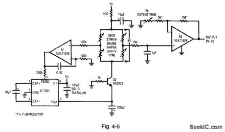
Figure 4-6 shows a high-resolution version of the Fig, 4-5 circuit. The Fig. 4-6 circuit uses a bipolar positive-to-negative converter, which has much lower output impedance. The biasing used permits 8 V to appear across the bridge, requiring the 100-mA capability of the LT1054 to sink about 24 mA. This increased drive results in a more favorable transducer-gain per slope, increasing the signal-to-noise ratio. LINEAR TECHNOLOGY, APPLICATION NOTE 43, P. 7. (View)
View full Circuit Diagram | Comments | Reading(765)
Single_supply_bridge_amplifier_with_common_mode_suppression
Published:2009/7/24 5:09:00 Author:Jessie
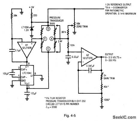
Figure 4-5 shows a circuit that is similar to that of Fig. 4-4, except that a single power supply is required. A2 biases the LTC1044 positive-to-negative converter. The LTC1044 output pulls the bridge output negative, causing the Al input to balance at 0 V. This local loop permits a single-ended amplifier (A2) to extract the bridge output signal. The 100-k℃/033-μF RC filter minimizes noise. The A2 gain is set to provide the desired output scale factor. Because bridge drive is taken from the LT1034 reference, the A2 output is not affected by supply shifts. The LT1034 output is available for ratio operation. Although the supply is 5 V, the transducer sees only 2.4 V of drive. This reduced drive results in lower transducer outputs for a given measurement value, effectively magnifying amplifier offset-drift terms. The limit on the available bridge drive is set by the CMOS LTC1044 output impedance. LINEAR TECHNOLOGY, APPLICATION NOTE 43, P. 7. (View)
View full Circuit Diagram | Comments | Reading(760)
VIDEO_AMPLIFIER_2
Published:2009/7/1 1:58:00 Author:May
View full Circuit Diagram | Comments | Reading(1362)
OTA_gain_control_amplifier
Published:2009/7/24 23:59:00 Author:Jessie
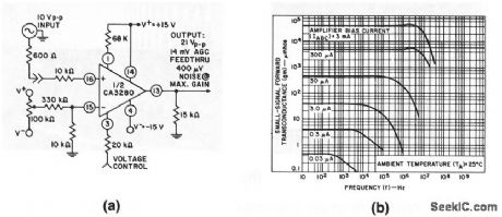
This circuit shows an OTA in a typical gain-control amplifier application. Figure 11-5B shows some typical characteristics. With an IABC of 1 mA,the gm is about 16 mmhos. With the CA3280 operating into a 5-KΩ resistor,the gain is 80. (View)
View full Circuit Diagram | Comments | Reading(831)
VIDEO_AMPLIFIER
Published:2009/7/1 1:58:00 Author:May
View full Circuit Diagram | Comments | Reading(0)
A_PRECISION_AMPLIFIER_WITH_DIGITALLY_PROGRAMMABLE_INPUTS_AND_GAIN
Published:2009/7/1 1:58:00 Author:May
View full Circuit Diagram | Comments | Reading(633)
OTA_sample_hold_circuit
Published:2009/7/24 23:58:00 Author:Jessie
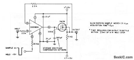
This circuit shows one section of an OTA combined with a JFET to form a sample-hold configuration. (View)
View full Circuit Diagram | Comments | Reading(860)
PROGRAMMABLE_AMPLIFIER
Published:2009/7/1 1:57:00 Author:May
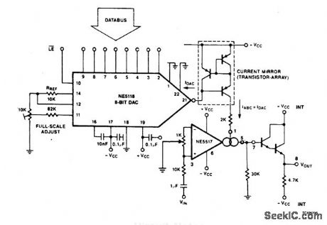
The intention of the following application shows how the NE5517 works in connection with a DAC. In the application, the NE5118 is used-an 8-bit DAC with current output-its input register making this device fully μP-compatible. The circuit consists of three functional blocks; the NE5118 which generates a control current equivalent to the applied data byte, a current mirror, and the NE5517. (View)
View full Circuit Diagram | Comments | Reading(1563)
JFET_BIPOLAR_CASCODE_VIDEO_AMPLIFIER
Published:2009/7/1 1:57:00 Author:May

The JFET-bipolar cascade circuit will provide full video output for the CRT cathode drive. Gain is about 90. The cascode configura-tion e liminate s Millercapacitance problems with the 2N4091 JFET, thus allowing direct drive from the video detector. An m-derived filter using stray capacitance and a variable inductor prevents 4.5 MHz sound frequency from being amplified by the video amplifier. (View)
View full Circuit Diagram | Comments | Reading(1725)
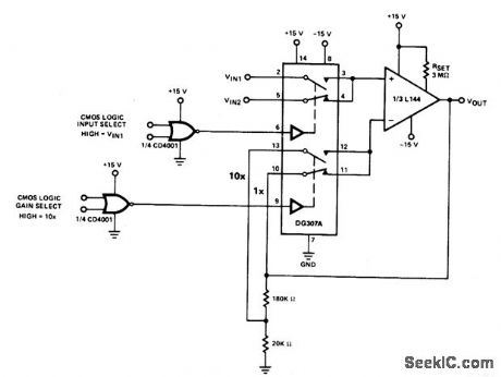
LOW_POWER_NON_INVERTING_AMPLIFIER_WITH_DIGITALLY_SELECTABLE_INPUTS_AND_GAIN
Published:2009/7/1 1:56:00 Author:May
View full Circuit Diagram | Comments | Reading(715)
LOW_POWER_BINARY_TO_10SUPn_SUP_GAIN_LOW_FREQUENCY_AMPLIFIER
Published:2009/7/1 1:55:00 Author:May
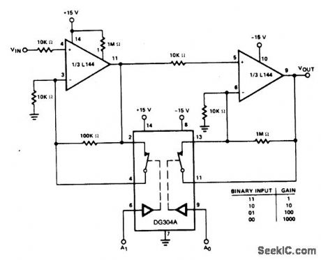
Gain increases by decades as the binary input decreases from 1,1 to 0,0. Minimum gain is 1 and maximum gain is 1000, Since the switch is static in this type of amplifier the power dissipation of the switch will be less than a tenth of a milliwatt. (View)
View full Circuit Diagram | Comments | Reading(629)
LOW_POWER_INVERTING_AMPLIFIER_WITH_DIGITALLY_SELECTABLE_GAIN
Published:2009/7/1 1:55:00 Author:May

View full Circuit Diagram | Comments | Reading(791)
HIGH_IMPEDANCE_LOW_CAPACITANCE_AMPLIFIER
Published:2009/7/1 1:50:00 Author:May
This compound series-feedback circuit provides high input impedance and stable,wide-band galn for general purpose video amplifier applications. (View)
View full Circuit Diagram | Comments | Reading(986)
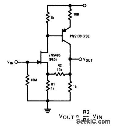
FET_CASCODE_VIDEO_AMPLIFIER
Published:2009/7/1 1:49:00 Author:May
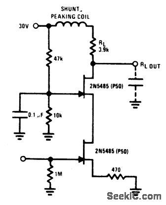
The FET cascode video amplifier features very low input loading and reduction of feed-back to almost zero. The 2N5485 is used be-cause of its low capacitance and high Yfs. Bandwidth of this amplifier is limited by R1, and load capacitance. (View)
View full Circuit Diagram | Comments | Reading(2096)
SATURATED_STANDARD_CELL_AMPLIFIER
Published:2009/7/1 1:04:00 Author:May
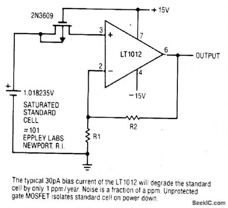
View full Circuit Diagram | Comments | Reading(670)
CURRENT_COLLECTOR_HEAD_AMPLIFIER
Published:2009/7/1 1:02:00 Author:May
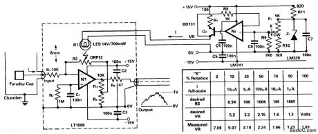
To amplify small current signals such as from an electron-collector inside a vacuum chamber, it is convenient for reasons of noise and bandwidth to have a head-amplifler: ' attached to the chamber. The op amp N1 is a precision bipolar device with extremely low bias current and offset voltage (1) as well as low noise, which allows the 100:1 feedback attenuator R4:R5. The resistance of R3 can be varied from above 10M to below 1R, and so the nominal 0 to 1 V-peak output signal corresponds to input current ranges of 1 nA to 10 μA, this current i enters via the protective resistor R1. Light from the bulb BI shines on R3, and the filament current I is controlled by the op amp N2.The reference voltage VR is shaped by the resistors R9R10 so as to tailor the bulb and LDR characteristics to the desired current ranges. Thus, rotation of the calibrated knob K gives the appropriate resistance to R3 for the peak-current scale shown. (View)
View full Circuit Diagram | Comments | Reading(819)
INSTRUMENT_PREAMP
Published:2009/7/1 0:59:00 Author:May
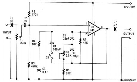
The input impedance is the value of potentiometer R1. If your instrument has extra-deep bass, change capacitor C1 to 0.5 μF. What appears to be an extra part in the feedback loop is a brightening tone control. The basic feedback from the op amp's output (pin 6) to the inverting input (pin 2) consists of resistor R7, and the series connection of resistor R4 and capacitor C3, which produce a voltage gain of almost 5 (almost 14 dB). That should be more extra oomph than usually needed. If the circuit is somewhat short on bass response, increase the value of capacitor C3 to 1 to 10μF. Start with 1 μF and increase the valud until you get the bass effect you want. (View)
View full Circuit Diagram | Comments | Reading(1942)
THERMALLY_BASED_ANEMOMETER(AIR_FLOWMETER)
Published:2009/7/1 0:32:00 Author:May
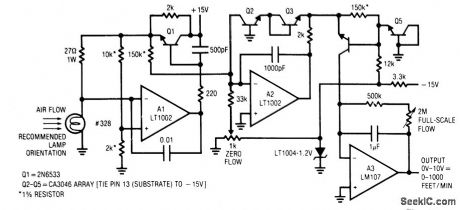


This design used to measure air or gas flow works by measunng the energy required to maintain a heated resistance wlre at constant temperature. The positive temperature coefficient of a small lamp,in combination with its ready availability,makes it a goodsensor,A type 328 lamp is modified for this circuit by removlng its glass envelope,Thelamp IS placed h a bridge whichis monitored by A1. A1's output iS current amplifiedby Q1 and fed back to drive the bridge,When power IS applied,the lamp IS at a lowresistance and Q1's emitter tries to come fun on.As current flows through the lamp,its temperature quickly rises,forcing its resistance to increase.This action increasesA1's negative input potential.Q1's emltter voltage decreases and the circuit finds a stableoperating point.To keep the bridge balanced,A1 acts to force the lamp's resistance,hence its temperature,constant,The 20 k - 2 k bridge values have been chosen so that the lamp operates just below the incandescence point.To use this circuit,place the lamp in the air flow so that its filament is at a 90°angle to the flow.Next,either shut off the air flow or shield the lamp from it and adjust the zero flow potentiometer for a circuit output of 0 V.Then,expose the lamp to air flow of 1000 feet/minute and trim the full flow potentiometer for 10 Ⅴ output.Repeat these adjustments until both points are fixed.With this procedure completed,the air flowmeter iS accurate within 3%over the entire 0-1000 foot/minute range.
(View)
View full Circuit Diagram | Comments | Reading(1517)
PHOTODIODE_SENSOR_AMPLIFIER
Published:2009/6/30 23:57:00 Author:May
View full Circuit Diagram | Comments | Reading(1144)
| Pages:135/250 At 20121122123124125126127128129130131132133134135136137138139140Under 20 |
Circuit Categories
power supply circuit
Amplifier Circuit
Basic Circuit
LED and Light Circuit
Sensor Circuit
Signal Processing
Electrical Equipment Circuit
Control Circuit
Remote Control Circuit
A/D-D/A Converter Circuit
Audio Circuit
Measuring and Test Circuit
Communication Circuit
Computer-Related Circuit
555 Circuit
Automotive Circuit
Repairing Circuit