
Amplifier Circuit
Index 122
PT8A2621 Infrared Induction Lamp Controlled Intergrated Circuit
Published:2011/7/23 2:51:00 Author:Michel | Keyword: Infrared Induction, Lamp Controlled, Intergrated Circuit
PT8A2621 is large-scale integrated circuit with CMOS technology produced by PT company.It is mainly used in the infrared inductive movement of human body lamp control.The PT8A2621 uses relay control method, which can be widely used in the corridor, kitchen,courtyard, conference room, warehouse, the energy saving of lighting handicraft etc.
First,Pins Functions and Inside Circuit Block Circuit
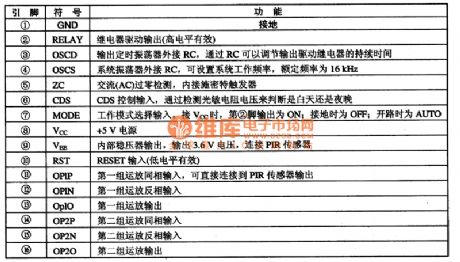
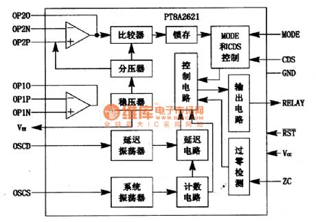
PT8A2621 has 16 feet DP or SDP package and its pins functions are shown as table.Its inside circuit block diagram of intergrated circuit is shown as picture 1.
Table 1: PT8A2621 Pins Functions
Second,Typical Application Circuit
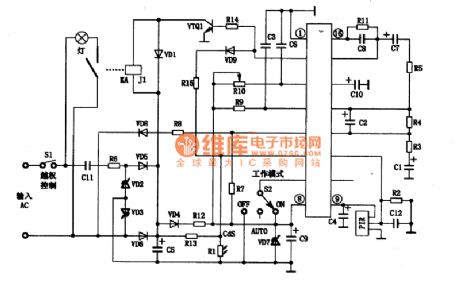
Typical application circuit of PT8A2621 is shown as picture 2.The S1 switch in the figure is used as excessive control.The voltage is provided by rectifier voltage regulating circuit and relay KAJ1 is used to control the lamp.
(View)
View full Circuit Diagram | Comments | Reading(883)
STK3048+SAP15N/P Power Amplifier Circuit Restructured From The Original Board
Published:2011/8/2 5:02:00 Author:Robert | Keyword: Power Amplifier, Restructure, Original, Board
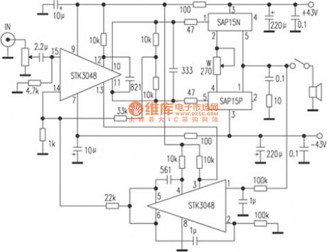
The features of this power amplifier are listed here:1.It needn't to make printed board by yourself and it would be easy to restructure. 2.It has no large loop circuit negative feedback and this would improve the transient response. 3.The middle point outputs DC servo to make the middle point's voltage be zero all the way. 4.Its static current could be adjusted anyway which depends on the user's favor. 5.Its front and back stages can be suit for one group of power supply and it needs not to add other transistors. The circuit is simple.
The new audio large-power tube SAP15N/P's package is single in-line 5-pin package. It has built-in temperature compensation diode, push tube, end large-power tube and emitter polar large-power resistor. (View)
View full Circuit Diagram | Comments | Reading(2791)
SYNCHRONOUS_SAMPLER
Published:2009/7/23 22:00:00 Author:Jessie
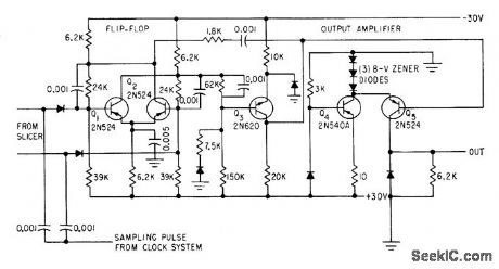
Time jitter of digital receiver output pulse is eliminated by synchronous sampling of detected signal. Each bit is sampled by local clock pulses that trigger flip-flop Q1-Q2. Two outputs of slicer, 180° out of phase, are applied to bases of Q1 and Q2. Output of flip-lop is regenerated information, free of jitter.-J. L. Hollis, Sending Digital Data Over Narrow. Band Lines, Electronics, 32:23, p 72-74. (View)
View full Circuit Diagram | Comments | Reading(641)
HYDROPHONE_PREAMPLIFIER
Published:2009/7/23 21:59:00 Author:Jessie
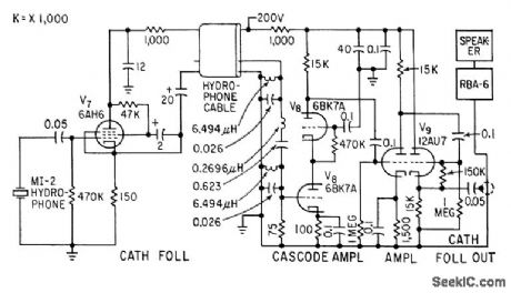
Cathode-follower hydrophone isolation amplifier and high-gain preamplifier feed Navy RBA-6 low-frequency radio receiver on trawler, to receive modulated 21-kc beam that transmits trawl net depth data.-F. H. Stephens, Jr., Underwater Telemeter for Trawl Fishing, Electronics, 32:13, p 66-68. (View)
View full Circuit Diagram | Comments | Reading(970)
Tuned_amplifier_CM_pinout
Published:2009/7/23 21:57:00 Author:Jessie
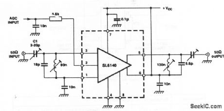
This circuit shows an SL6140 connected as a single-ended amplifier with tuned input and output networks (Fig. 2-40). The bandwidth and gain depend on the Q of the tuned/matching circuits. Using the values shown, the bandwidth is 100 MHz, with a power gain of 35 dB. (View)
View full Circuit Diagram | Comments | Reading(753)
Photodiode_amplifier_1
Published:2009/7/23 21:57:00 Author:Jessie
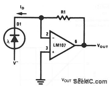
As shown by the equation,VOUT depends on photodiode current and R1 (which should be chosen for range or scale factor). (View)
View full Circuit Diagram | Comments | Reading(644)
Gentleman E1080PK Decoding Power Amplifier Upgrading Circuit
Published:2011/7/26 21:11:00 Author:Robert | Keyword: Gentleman, Decoding, Power Amplifier, Upgrading
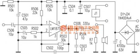
The picture shows the Gentleman E1080PK decoding power amplifier upgrading circuit.
1.In the original device the middle power amplifier and the surrounding power amplifier have the same principle which are installed on a same circuit board (which is shown in the picture). The difference is the surrounding power amplifier's negative feed-back resistance R60 is 150kΩ. So it should also change the feed-back resistance R503 to 150kΩ in the middle power amplifier to make the dual sound-channels' gain be same. The original device's middle power amplifier would be used as another sound-channel surrounding power amplifier. And also it should make the original device's four surrounding wiring terminals's series terminals be disconnected and then connect them to the dual channel surrounding power amplifier's output ports. (View)
View full Circuit Diagram | Comments | Reading(537)
OTL Power Amplifier Principle Circuit
Published:2011/7/29 18:41:00 Author:Robert | Keyword: OTL, Power, Amplifier, Principle
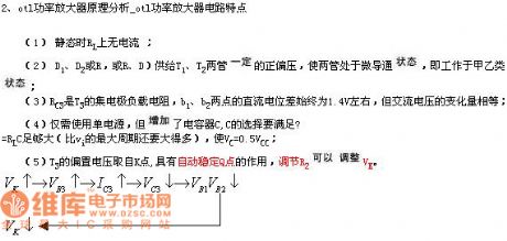
2.The analysis for otl power amplifier principle.
The features of the otl power amplifier are listed here.
(1)When static there is no current through RL.
(2)D1, D2 or R, or R, D, would supply the T1, T2 two transistors a certain positive bias voltage to make them in micro-conduction mode, which means working in class AB.
(3)RC3 is T3's collector polar's load resistance. b1, b2 these two points' voltage difference is about 1.4V all the way. But their AC voltage's variation values are the same.
(4)When it only needs a single power and it also adds a capacitor C, the selection of C should meet:C should be large enough (larger than Vi's maximum cycle time) to make Vc=0.5Vcc.
(5)T3's bias voltage is get from the K point. It has the function that make the Q point stable automatically and it could adjust the Vk by adjusting R2. (View)
View full Circuit Diagram | Comments | Reading(568)
Serially_programmable_VHF_frequency_synthesizer
Published:2009/7/23 22:15:00 Author:Jessie
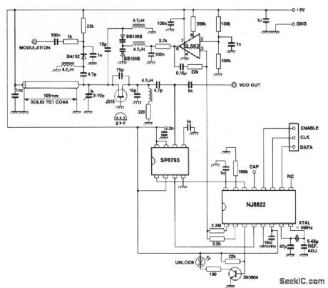
This circuit uses an NJ8822 single-chip synthesizer, an SP8793 dual-modulus prescaler, and an SL562 op amp. The VCO is a JFET oscillator that uses a transmission line as the resonator. This VCO is modulated by applying the audio signal to the cathode of a reverse-biased PIN diode, as shown in the circuit diagram. The loop filter uses the SL562, which (with the values shown) has a loop bandwidth of 60 Hz and a damping factor of 0.6. This filter is followed by a low-pass pole at 3.7 kHz to attenuate the 12.5-kHz reference sidebands. The lock-up time for a 1-MHz change in frequency is 80 ms. The output frequency range is 144 to 146 MHz and the level is +3 dB into 50Ω. (View)
View full Circuit Diagram | Comments | Reading(3241)
400_Hz_SERVO_AMPLIFIER
Published:2009/7/5 21:47:00 Author:May
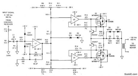
The signal from a synchro receiver or a variable resistive cam follower (potentiometer) is boosted by operational amplifier U1, whose output swing is limited by back-to-back zeners D3 and D4. The signal is then applied to operational amplifiers U2 and U3, which drive the gates of Q1 and Q2 respectively. The npn transistor (Q3) is a fast current limiter for the n-channel MTM8N10; a pnp transistor (Q4) performs the same function for the p-channel MTM8P10. Capacitors C3 and C4 eliminate the need for accurate dc offset zeroing. T1 steps up the output voltage to 120 V for the 400 Hz servo motor. (View)
View full Circuit Diagram | Comments | Reading(2079)
TIME_INTERVAL_ANALYZER
Published:2009/7/23 22:09:00 Author:Jessie
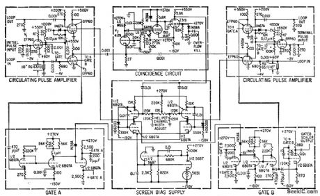
Gives high resolution (better than 1 millimicrosec) for multichannel measurements of short-life nuclear particles. Two pulses, defining time interval, are fed into the same loop-forming ends of two transmission lines. By making coincidence circuit spacing slightly smaller on terminal pulse lines than on initial pulse lines, terminal pulse is made to overtake initial pulse. Pulses approach coincidence al 1 millimicrosec per transit, so count of transits before coincidence gives time interval-H. W. Lefevre and J. T. Russell, Vernier Chronotron limes Nuclear Particle Flight, Electronics, 32:10, p 44-47. (View)
View full Circuit Diagram | Comments | Reading(929)
S25610 Microcomputer Dialing Integrated Circuit
Published:2011/7/29 3:18:00 Author:Michel | Keyword: Microcomputer Dialing, Integrated Circuit
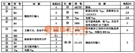
S25610 is system microcomputer dialing integrated circuit that is widely used in communication telephone circuit.
First,Functions FeaturesS25610 integrated circuit contains pulse dialing generating circuit, key switch signal decoding circuit, the noise and static control circuits etc.
Second,Pins Functions and DataS25610 adopts feet 18 DIP generating circuit and its pins functions and data are shown as table 1.
Table 1:S25610 IC Pins Functions and Data (View)
View full Circuit Diagram | Comments | Reading(561)
CX20106/CX20106A (TV) infrared remote control receiving preamplifier circuit
Published:2011/8/1 8:16:00 Author:Christina | Keyword: TV, infrared, remote control, receiving, preamplifier circuit
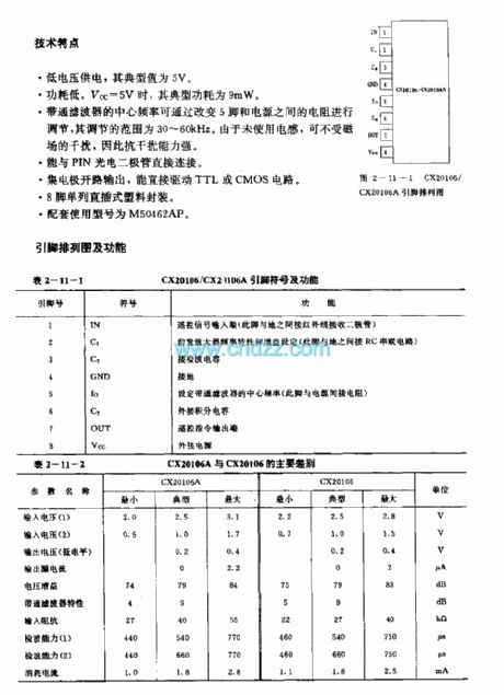
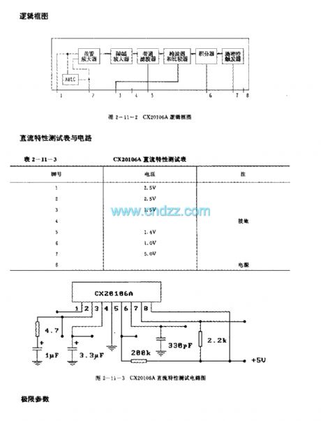
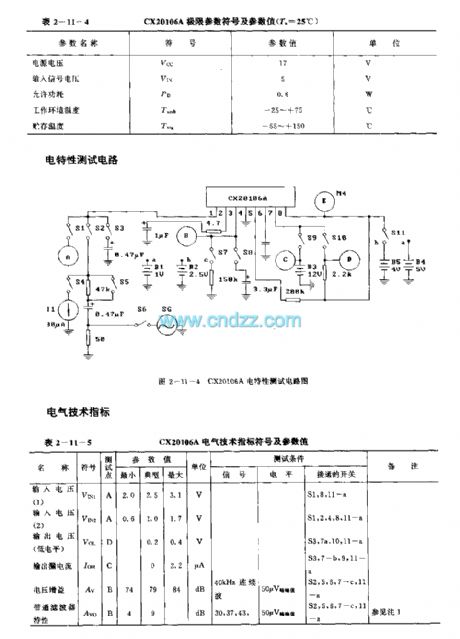
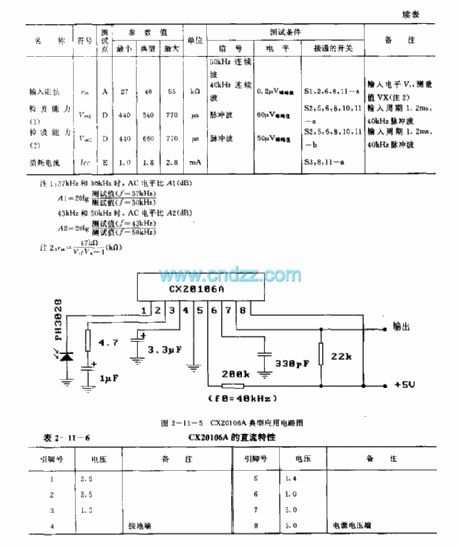
The CX20106/CX20106A is designed as the infrared remote control receiving preamplifier bipolarity circuit that can be used in the TV application. The internal circuit is composed of the preamplifier, the ABLC, the amplitude limiting amplifier,the bandpass filter, the peak value wave detector and the waveform shaping circuit. The CX20106A is the improved model of CX20106, the difference between the CX20106 and CX20106A is the electrical parameter.
Features
Low power voltage, the typical value is 5V.Low power consumption. When Vcc=5V, the typical power consumption is 9mW.You can change the centre frequency of the bandpass filter by changing the resistance between the pin-5 and the power supply.It can be connected with the PIN photoelectric diode. It is in the 8-pin single row DIP plastic package.The matching model is M50462AP.
(View)
View full Circuit Diagram | Comments | Reading(3434)
S14133-MLP28 Frequency Synthesizer Integrated Circuit
Published:2011/7/29 2:16:00 Author:Michel | Keyword: Frequency Synthesizer, Integrated Circuit
(View)
View full Circuit Diagram | Comments | Reading(585)
BA6340 (VCR) infrared remote control receiving preamplifier circuit
Published:2011/8/1 8:08:00 Author:Christina | Keyword: VCR, infrared, remote control, receiving, preamplifier circuit
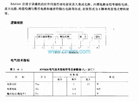
The BA6340 is designed as the infrared remote control receiving preamplifier circuit that can be used in the VCR application. The internal circuit is composed of the receiving circuit, the amplifier circuit, the peak value detection circuit, the shaping circuit and the Schmidt output circuit. This device is in the 8-pin single row DIP plastic package.
(View)
View full Circuit Diagram | Comments | Reading(645)
HD44042 (TV) infrared remote control receiving preamplifier circuit
Published:2011/8/1 3:03:00 Author:Christina | Keyword: TV, infrared, remote control, receiving, preamplifier circuit
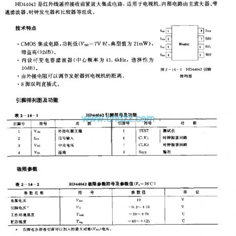
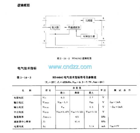
The HD44042 is designed as the infrared remote control receiving preamplifier circuit that can be used in the TV application. The internal circuit is composed of the main amplifier, bandpass filter, clock generator and the comparator.
Features
It uses the CMOS integrated circuit, the power consumption is low (when the VDD=7V, the typical value is 21mW), the gain is high (92dB).It has the variable capacity filter (the center frequency is 41.4kHz, the gain is 10dB).The external resistance can change the distance between the transmitter and the television.8-pin dual-row DIP package.
(View)
View full Circuit Diagram | Comments | Reading(761)
15_W_AM_amplifier
Published:2009/7/23 22:58:00 Author:Jessie
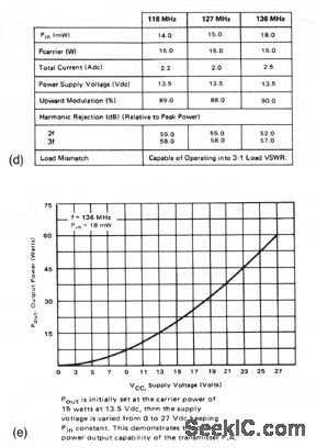
This circuit is a 15-W AM broadband amplifier covering the 118- to 136-MHz aircraft band. Figure 2-52B shows the details for T1, and Fig. 2-52C shows a series modulator that is suitable for testing or modulating the amplifier.Figure 2-52D shows amplifier performance and Fig. 2-52E shows output power versus supply voltage.
(View)
View full Circuit Diagram | Comments | Reading(673)
MAGNETOSTRICTIVE_DELAY_LINE_AMPLIFIER
Published:2009/7/23 22:56:00 Author:Jessie
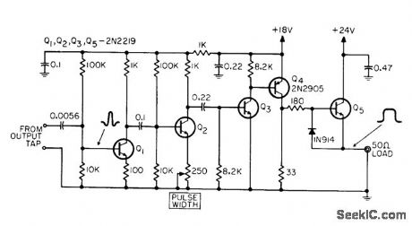
Used to reshape output signal of delay line used as 12-event serializer. Q3 clips two negative peaks of signal and Q4 fattens pulse. Pulse width control adjusts gain of Q2 to vary pulse width.-R. P. Rufer, How to Measure Simultaneous Events with Magneto-strictive Delay Lines, EEE, 14:5, p 44-49. (View)
View full Circuit Diagram | Comments | Reading(901)
CONSTANT_BANDWIDTH_AMPLIFIER
Published:2009/7/5 20:54:00 Author:May

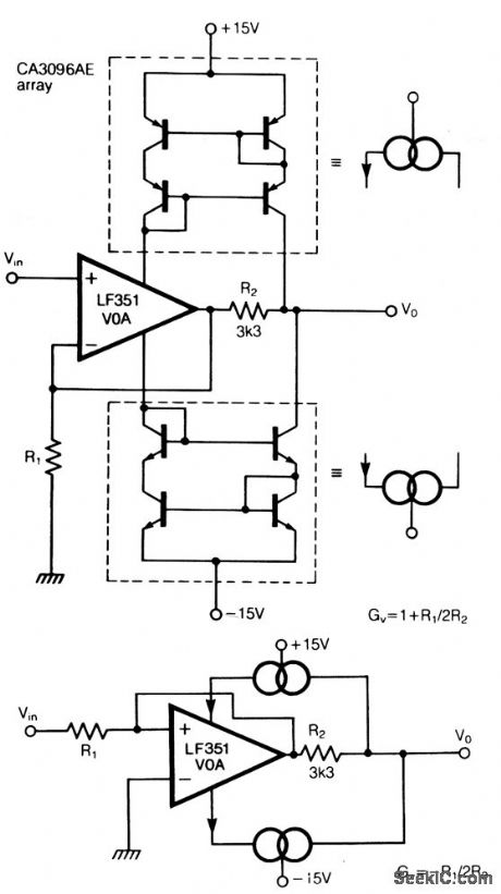
The traditional restriction of constant gainbandwidth products for a voltage amplifter can be overcome by employing feedback around a current amplifier. Two current mirrors, constructed from transistors in a CA3096AE array, effectively turn the LF351 op amp into a current amplifter. Feed-back is then applied by using R2 and R1, turning the whole circuit into a feedback voltage amplifier with a noninverting gain of G of 1 + R1 /2R2.
Using the values shown, a constant bandwidth of 3.5 MHz is obtained for all voltage gains up to and beyond 100 at 10 V pk-pk output, equivalent to a gain-bandwidth product of 350 MHz from an op amp with an advertised unity gain-bandwidth of 10 MHz. An inverting gain conftguration is also possible (see Fig. 2) where G = R1/2R2. Slewing rates are signiftcantly improved by this approach; even a 741 can manage 100 V μs under these conditions since its output is a virtual earth. However, because the new conftgurations use current feedback to achieve bandwidth independence, an output buffer should be added for circuits where a significant output current is required.
(View)
View full Circuit Diagram | Comments | Reading(861)
CURRENT_SHUNT_AMPLIFIER
Published:2009/7/5 20:52:00 Author:May
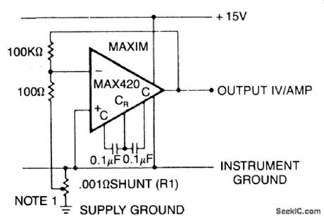
This circuit measures the power-supply current of a circuit without really having a currentshunt resistor: R1 is only 3 cm of #20 gauge copper wire. A length of the power distribution wiring can be used for R1. The MAX420's CMVR includes its own negative power supply; therefore, it can both be powered by and measure current in the ground line. (View)
View full Circuit Diagram | Comments | Reading(1062)
| Pages:122/250 At 20121122123124125126127128129130131132133134135136137138139140Under 20 |
Circuit Categories
power supply circuit
Amplifier Circuit
Basic Circuit
LED and Light Circuit
Sensor Circuit
Signal Processing
Electrical Equipment Circuit
Control Circuit
Remote Control Circuit
A/D-D/A Converter Circuit
Audio Circuit
Measuring and Test Circuit
Communication Circuit
Computer-Related Circuit
555 Circuit
Automotive Circuit
Repairing Circuit