
Amplifier Circuit
Index 141
1_W_INVERTING
Published:2009/6/29 3:11:00 Author:May
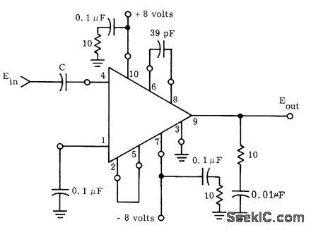
Uses Motorola MC1554 power amplifier to provide voltage gain of 35 with componentsshown. Output voltageswing is 12 V P-P into 12-ohm load. For responsedown to low audio frequencies (below 100 Hz), large value of C is required, such as 1μF. Input can be direct-coupled at sacrifice in output offset, but this can be corrected by properly biasing pin 1 or terminating it in about 250 ohms. Upper fre-quency limit for -3 dB is about 22,000 Hz.-' The MC1554 One-Watt Monolithic Integrated Circuit Power Amplifier, Motorola, Phoenix, AZ, 1972, AN.401, p 3. (View)
View full Circuit Diagram | Comments | Reading(691)
5_W_WITH_OPAMP
Published:2009/6/29 2:54:00 Author:May
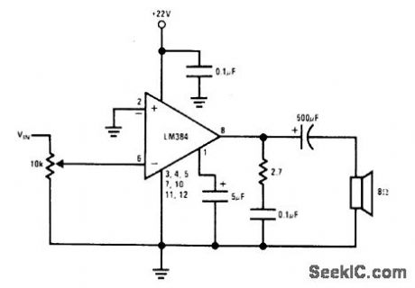
Simple circuit including volume control has low harmonic distortion.Higher allowable operating voltage of LM384 opamp gives higher output power, but heatsink is required.- Audio Handbook, National Semiconductor, Santa Clara, CA, 1977, p 4-28-4-29. (View)
View full Circuit Diagram | Comments | Reading(891)
ERROR_ADD_ON_REDUCES_DISTORTION
Published:2009/6/29 2:54:00 Author:May
Based on fact that error at output of upper opamp also appears at input of this opamp, Error signal is taken from this input for lower opamp, where it is amplified by opamp and Darlington for addition to output of upper Darlington. Article gives design equations and intimates that open-loop gain improves at 12 dB per octave as compared to conventional 6 dB, Applications include reduction of loudspeaker distortion which cannot be handled by negative feedback.-A.Sandman, Reducing Distortion by 'ErrorAdd-On.' Wireless World, Jan. 1973, p 32. (View)
View full Circuit Diagram | Comments | Reading(783)
High_stability_thermocouple_amplifier
Published:2009/7/24 22:16:00 Author:Jessie
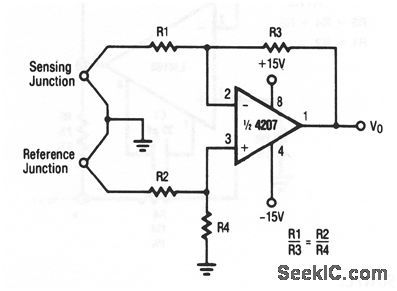

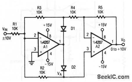
Notice that the reference-junction output is applied to the noninvert-ing input of the 4207, and the sensing-junction output is applied to the inverting input. See chapter 13 for additional temperature sensing and control circuits. (View)
View full Circuit Diagram | Comments | Reading(0)
BRIDGE_AMPLIFIER
Published:2009/6/29 2:40:00 Author:May
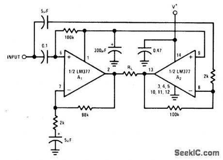
National LM377 dual power amplifieris used in bridge configurationto drive floating load that can be loudspeaker servomotor, or other device having impedance of 8 or 16 ohms,Maximum outputis 4 W at gain of 40 dB with 3-dB response extending fromabout 20 Hz to above 100 kHz.-″Audio Hand-book″ National Semiconductor、 Santa Clara、CA,1977、p 4-8-4-20. (View)
View full Circuit Diagram | Comments | Reading(0)
Wien_bridge_oscillator_with_fed_amplitude_stabilization
Published:2009/7/24 22:14:00 Author:Jessie
This circuit is similar to that of Fig. 10-22, except that a lamp is not used, and the output is stabilized in amplitude by a 2N3819 FET. (View)
View full Circuit Diagram | Comments | Reading(1520)
90_W_PER_CHANNEL
Published:2009/6/29 2:33:00 Author:May
Combination of LM143 highvoltage opamp and curent booster can provide up to 90 WRMS into 4-ohm Ioudspeaker or 70 WRMS into 8-ohm Ioudspeaker. Circuit features indude shortcircuit and overload protection along with harmonic distortion below 0.1% at 1 kHz. Transistors Q1-Q4 should be on common Thermalloy 6006B or equivalent heat-sink.- Linear Applications, Vol. 2, National Semiconductor, Santa Clara, CA, 1976, AN-127, p 6-7. (View)
View full Circuit Diagram | Comments | Reading(916)
Power_op_amp_with_parallel_output
Published:2009/7/24 23:14:00 Author:Jessie
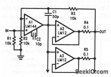
This circuit shows two LM12s (Fig. 10-46) connected in parallel to increase the load-current capability. (View)
View full Circuit Diagram | Comments | Reading(811)
Power_op_amp_follower_inverter
Published:2009/7/24 23:13:00 Author:Jessie
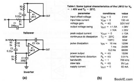
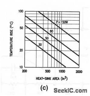
This circuit shows an LM12 power op amp connected as both a follower and an inverter, with input compensation to reduce bandwidth and increase stability. Figure 10-46B shows typical characteristics for the LM12, which is compensated for unity-gain feedback, and a small-signal bandwidth of 700 kHz. The LM12 is housed in a TO-3 package and requires a heatsink (because of the high power). Figure 10-46C shows the heatsink surface area required for temperature rise and power dissipation. National
(View)
View full Circuit Diagram | Comments | Reading(882)
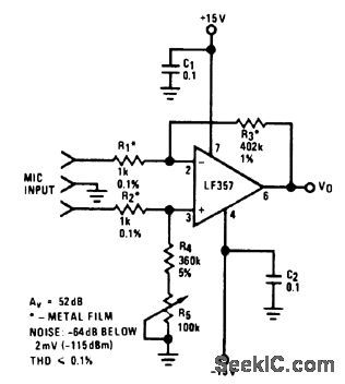
SINGLE_ENDED_MICROPHONE_PREAMP
Published:2009/6/29 2:32:00 Author:May
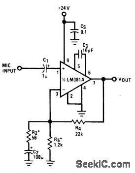
Noise performance is -69 dB below 2-mV input reference point. Use metal-film resistors for R2 and R5. Total harmonic distortion is less than 0.1%. Gain is set by ratio of R4 to R2 and is 52 dB.- Audio Handbook, National Semicon-ductor, Santa Clara, CA, 1977, p 2-37-2-40. (View)
View full Circuit Diagram | Comments | Reading(779)
VOLTAGE_WINDOW_COMPARATOR
Published:2009/6/29 2:32:00 Author:May
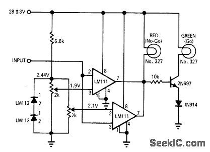
Use of LM111 opamps minimizes number of components required to turn on green indicator Iamp when input voltage is between predetermined limits set by 2K pots. Similar circuit using 741 opamps requires total of 31 components. Improved eircuit draws only 120 nA from voltage level being monitored, and operates within 0.3% threshold level stability using single unregulated supply varying ±3 V from 28 V.—D. Priebe, Comparators Compared, EDN|EEE Magazine, Oct. 1, 1971, p 61, (View)
View full Circuit Diagram | Comments | Reading(2723)
Op_amp_instrumentation_amplifier_with_adjustable_gain
Published:2009/7/24 23:07:00 Author:Jessie
This circuit is similar to that of Fig. 10-35, except that the voltage gain can be adjusted (from 1 to 300) by selection of R6. With the values shown for R2/R4 and R3/R5, CMRR is 60 dB. (View)
View full Circuit Diagram | Comments | Reading(925)
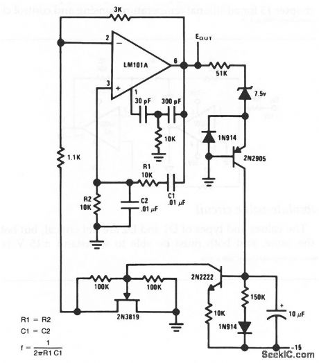
Feedforuoard_compensation_to_speed_op_amp_response
Published:2009/7/24 23:05:00 Author:Jessie
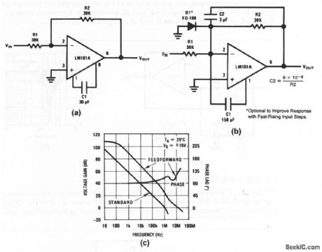


The slew rate and bandwidth of most op amps can be increased using feedforward compensation. Figure 10-44A shows an LM101A with standard compensation, while Fig. 10-44B shows feedforward compensation. Figure 10-44C shows a comparison of the two methods. Feedforward is accomplished by connecting C1 between the inverting input and one of the compensation pins (to eliminate internal pnps from the signal path at high frequencies). Unity gain bandwidth is extended from about 1 to 10 MHz, while the slew rate is increased from about 0.5 to 10 V/μS. (View)
View full Circuit Diagram | Comments | Reading(880)
True_rms_detector
Published:2009/7/24 23:00:00 Author:Jessie
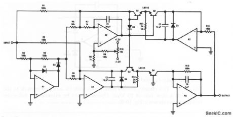
This circuit provides a dc output equal to the rms value of the input. Accuracy is typically 2% for a 20-V pp input from 50 Hz to 100 kHz. To calibrate, apply 10 Vdc at the input, and adjust R10 for 10V dc at the output.Q1 through Q4 should be matched, have high beta, and all mounted on a common heatsink. Bypass all Op amp supplies with 0.1-μF disc capacitors. (View)
View full Circuit Diagram | Comments | Reading(3686)
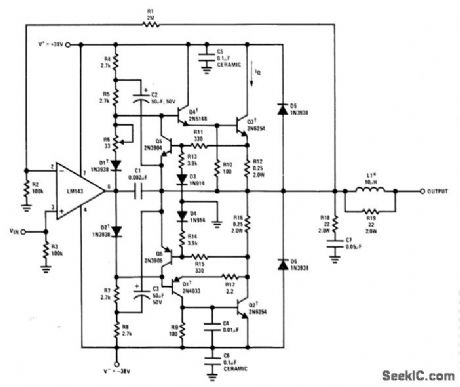
75_W_WITH_CURRENT_LIMITING
Published:2009/6/29 2:27:00 Author:May
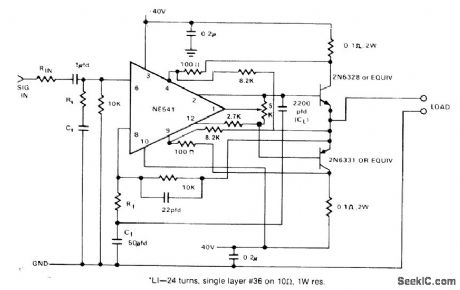

Signetics NE541 high-voltage power amplifier provides current gain of 90 dB from 20 Hz to 20 kHz andoutput levels up to 20 VRMS from 300-mVRMS input.IC includes built-in short-circuit protection,with additional protection provided by external current limiting,Transistors in output stage boost power to 75 W for driving loud-speaker load.- Signetics Analog Data Manual, Signetics, Sunnyvale, CA, 1977, p 765 (View)
View full Circuit Diagram | Comments | Reading(1338)
OTA_four_quadrant_multiplier
Published:2009/7/24 23:51:00 Author:Jessie
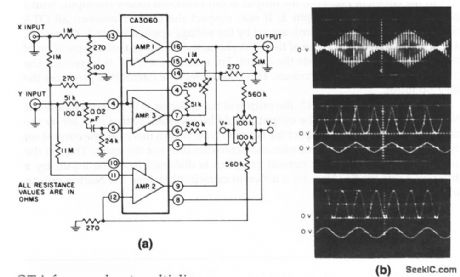
This circuit uses all three sections of an OTA to form a four-quadrant multiplier. To adjust the circuit, remove all signals from the X and Y inputs, connect pin 10 to pin 8 (to disable amp 2), and set the Amp 1 offset to zero with the 100-kΩ potentiometer (adjust the pot until the output is zero). Disconnect pin 10 from pin 8, and connect pin 15 to pin 8 (to disable amp 1), and set the Amp 2 offset to zero with the corresponding 100-kΩ pot (adjust the pot until the output is zero). Disconnect pin 15 from pin 8. Apply equal ac signals to both the X and Y inputs. Adjust the 100-Ω and 200-kΩ pots for symmetrical output signals. Figure 11-2B shows the output waveform with the multiplier adjusted. The voltage waveform in Fig. 11-2Ba shows suppressed-carrier modulation of the 1-kHz carrier with a triangle wave. Figures 11-2Bb and 11-2Bc, respectively, show the squaring of a triangular wave and a sine wave. Notice that in both cases, the output are always positive and return to zero after each cycle. (View)
View full Circuit Diagram | Comments | Reading(2591)
Norton_peak_detector
Published:2009/7/24 23:48:00 Author:Jessie
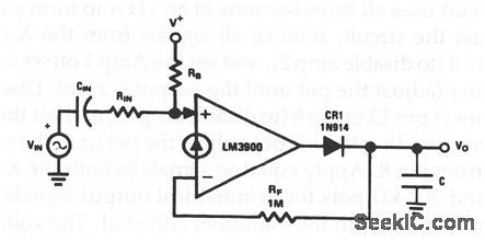
In this circuit, the Norton is used to rapidly charge capacitor C to peak value of Vin. The voltage drop across CR1 is placed within the feedback loop to prevent voltage losses and temperature drifts in the output voltage. The feedback resistor (RF) is kept small (1 MΩ) so that the 30-nA base current of the Norton will cause only a +30-mV error in output voltage VO. Feedback resistor RF is con-stantly loading C, in addition the current drawn by the circuitry which samples VO. Bias resistor RB allows a minimum dc voltage to exist across C. Overall circuit gain is set by the value of RIN in relation to RF. (View)
View full Circuit Diagram | Comments | Reading(722)
TRANSFORMERLESS_BALANCED_INPUT_MI_CROPHONE_PREAMP
Published:2009/6/29 2:26:00 Author:May
Uses FET-input opanlp to amplify differential signals while rejecting common-mode signals. Gain is set at 52 dB by ratio of R3 to R1. Input resistors R1 and R2 are made large compared to source impedance while being kept as small as possible, for optimum balance between input loading effects and low noise. Good compromise value is 10 times source impedance for R1 + R2.- Audio Handbook, National Semiconductor, Santa Clara, CA, 1977, p 2-37-2-40. (View)
View full Circuit Diagram | Comments | Reading(901)
CLASS_B_WITHOUT_TAKEOVER_DISTORTION
Published:2009/6/29 2:25:00 Author:May
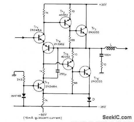
Circuit uses two transistor triplets in output stage, with quiescent current set at 15 mA by Tr7 which serves as constant-current source. For small signals, Tr1 and Tr4 can be regarded as long-tailed pair without tail. For positive signals, Tr1-Tr4 become active and behave as super emitter-follower, while Tr1 with Tr4-Tr6 serve for negative signals. One advantage of circuit is low output impedance.-N. M. Visch, A Novel Glass B Output, Wireless World, April 1975, p 166. (View)
View full Circuit Diagram | Comments | Reading(965)
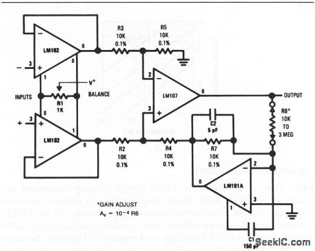
Precision_instrumentation_amplifier
Published:2009/7/24 23:25:00 Author:Jessie
This circuit provides differential-input to single-ended-output conversion with accurate circuit gain. Amplifier characteristics are shown in the table. (View)
View full Circuit Diagram | Comments | Reading(0)
| Pages:141/250 At 20141142143144145146147148149150151152153154155156157158159160Under 20 |
Circuit Categories
power supply circuit
Amplifier Circuit
Basic Circuit
LED and Light Circuit
Sensor Circuit
Signal Processing
Electrical Equipment Circuit
Control Circuit
Remote Control Circuit
A/D-D/A Converter Circuit
Audio Circuit
Measuring and Test Circuit
Communication Circuit
Computer-Related Circuit
555 Circuit
Automotive Circuit
Repairing Circuit