
Amplifier Circuit
Index 124
Tuned_amplifier_MP_pinout
Published:2009/7/23 22:35:00 Author:Jessie
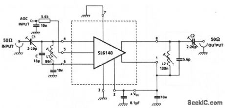
This circuit shows an SL6140 wideband AGC amplifier used as a 100-MHz tuned amplifier with a power gain of 35 dB (Fig 2-19). The high gain is achieved at the expense of bandwidth by means of the matching networks. L1 and L2 are adjusted to set the tuned frequency. C1 and C2 are adjusted to optimize gain.However, if too high an impedance is seen by the input or output, the circuit might oscillate. Adjust C1 and C2 for the minimum bandwidth necessary for the particular application. For best results, use a 50-Ω track ground plane from the matching networks to the 50-Ω source and load. (View)
View full Circuit Diagram | Comments | Reading(860)
PROM_BURNER
Published:2009/7/3 4:44:00 Author:May
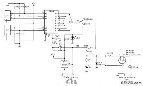
Meets radically different pro grahiming requirements for 8223 and 82S23 ROMs. S1 and S2 ale BCD thumbwheelswitches that select word address in octal. S3 select output bit to be programmed or verified.S4 is pushed momentarily to burn out programmed bit, and S5 verifies programming. S6 is set to PROM type, and S7 puts 12-V zeneracross 19-V zener for current calibration. For 82S23, adjust power suppliesto 10 and 21 V and adjust 25-ohm pot to give meter reading of 65mA when S7 is closed.-VV,J Hosking.Finally!A Simple PROM Burner! 73 Magazine, Dec.1977,p 186-187 (View)
View full Circuit Diagram | Comments | Reading(2156)
Instrumentation_amplifier_with_±_100_V_common_mode_range
Published:2009/7/23 22:34:00 Author:Jessie
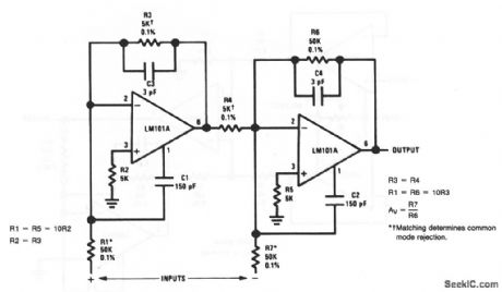
This circuit provides a much higher common-mode range than that of Fig.10-49,but has a lower input impedance. (View)
View full Circuit Diagram | Comments | Reading(835)
SUMMING_AMPLIFIER
Published:2009/7/3 4:34:00 Author:May
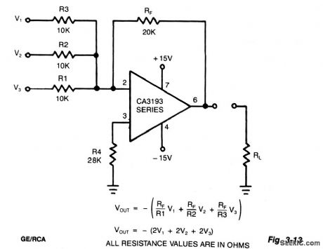
This circuit uses a CA3193 BiMOS op amp.Because mput nolse of the amplifier is increased by RF/R1//R2//R3,nd the gam that a single input will amplify is the gam of only one of the input channels (RF/R1),for good noise performance,use the smallest number of inputs. (View)
View full Circuit Diagram | Comments | Reading(0)
POLARITY_REVERSING_LOW_POWER_AMPLIFIER
Published:2009/7/3 4:33:00 Author:May
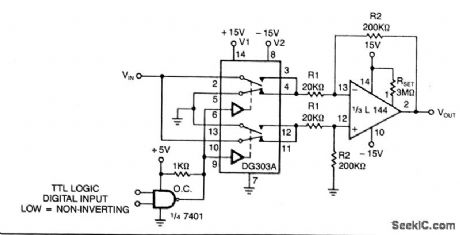
View full Circuit Diagram | Comments | Reading(626)
High_input_impedance_instrumentation_amplifier
Published:2009/7/23 22:27:00 Author:Jessie
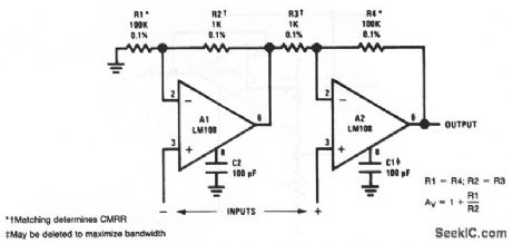
Compare this circuit to that of Fig,10-38 and 10-49. (View)
View full Circuit Diagram | Comments | Reading(0)
WIDE_BAND_AGC_AMPLIFIER
Published:2009/7/3 4:31:00 Author:May

The NE592 is connected in conjunction with a MC1496 balanced modulator to form an excellent auto-matic gain control system. The signal is fed to the signal input of the MC1496 and rc-coupled to the NE592. Unbalancing the carrier input of the MC1496 causes the signal to pass through unattenuated. Rec-tifying and filtering one of the NE592 outputs produces a dc signal which is proportional to the ac signal amplitude. After ftltering, this control signal is applied to the MC1496, causing its gain to change. (View)
View full Circuit Diagram | Comments | Reading(4950)
Instrumentation_amplifier_with_±_10_V_common_mode_range
Published:2009/7/23 22:26:00 Author:Jessie
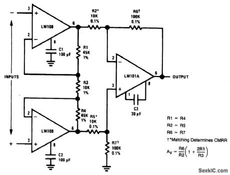
Compare this circuit to that of Fig,10-38. (View)
View full Circuit Diagram | Comments | Reading(713)
Bridge_amplifier_with_low_noise_compensation
Published:2009/7/23 22:29:00 Author:Jessie
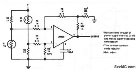
Compensating capacitor C1 makes supply bypassing unnecessary. (View)
View full Circuit Diagram | Comments | Reading(0)
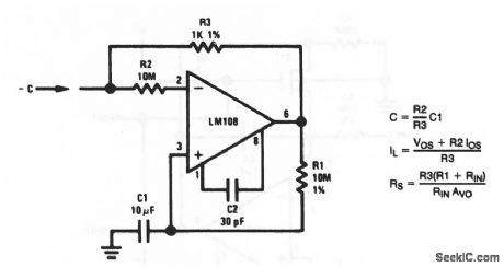
Simulated_inductor
Published:2009/7/23 22:39:00 Author:Jessie
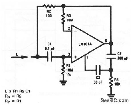
This circuit appears as an inductor to the input. The inductance is set by selection of R1, R2, and C1. (View)
View full Circuit Diagram | Comments | Reading(2702)
Amplitude_modulator
Published:2009/7/23 22:42:00 Author:Jessie
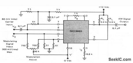
This circuit shows an MC1596 operating as an amplitude modulator with +12,- and -8-V supplies. The circuit provides modulation at any percentage from zero to greater than 100%. (View)
View full Circuit Diagram | Comments | Reading(0)
Linear_thermometer
Published:2009/7/23 22:42:00 Author:Jessie
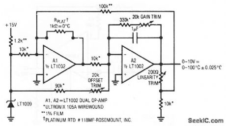
This circuit uses both sections of an LT1002 to form a simple (but accurate) thermometer. To calibrate, substitute a precision decade box (General Radio 1432-K) for the sensors. Set the box to the 0°C value (1000.0Ω) and adjust the offset trim for a 0.000-V output. Then, set the decade box for a 35°C output (1138.7 Ω) and adjust the gain trim for a 3.500-V output reading. Finally, set the box to 1392.6 Ω (100.00°C) and trim the linearity adjustment. Repeat the sequence until all three points are fixed. The total error over the entire range will be within ±0.025°C. (View)
View full Circuit Diagram | Comments | Reading(740)
Negative_variable_voltage_reference_VSUBOUT_SUB_lower_than_reference_zener
Published:2009/7/23 22:24:00 Author:Jessie
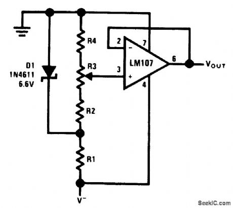
This circuit is similar to that of Fig.10-47,except that a variable negative-voltage reference is provided for VOUT . (View)
View full Circuit Diagram | Comments | Reading(669)
900_MHz_gain_controlled_amplifier
Published:2009/7/23 22:24:00 Author:Jessie
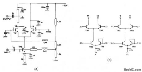
This circuit shows an SL2365 transistor array connected as a gain-controlled amplifier. The transistor-array connections are shown in Fig. 2-35B.The collector load of TR1 is a transformer that is composed of a 14-mm length of 75-Ω stripline resonated with a 1- to 6-pF variable capacitor. The transformer secondary is a small loop of stiff wire that is grounded at one end and located a few mm above the stripline. The noise figure at full gain is 9 dB. (View)
View full Circuit Diagram | Comments | Reading(1092)
Variable_gain_differential_input_instrumentation_amplifier
Published:2009/7/23 22:32:00 Author:Jessie
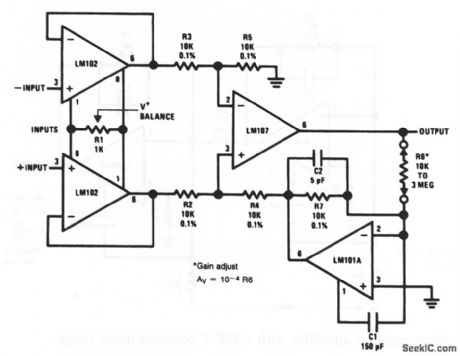
The gain of this instrumentation amplifier can be set by selecting R6. The amplifier can be balanced by adjusting R1. (View)
View full Circuit Diagram | Comments | Reading(0)
SONAR_THUMPER
Published:2009/7/23 22:38:00 Author:Jessie
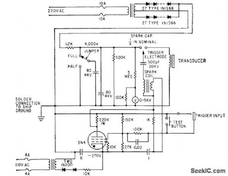
Strobotron tube circuit energizes spark coil, ionizing spark gap and discharging bank of 4,000-v capacitors through underwater transducer coil, causing adjacent aluminum plate to produce high-power sound pulse that penetrates sediment layers and bedrock for oceanographic research.-New Sonar Thumper Charts Ocean Subbottom, Electronics, 34:5, p 56:57. (View)
View full Circuit Diagram | Comments | Reading(760)
Variable_capacitance_multiplier
Published:2009/7/23 22:38:00 Author:Jessie
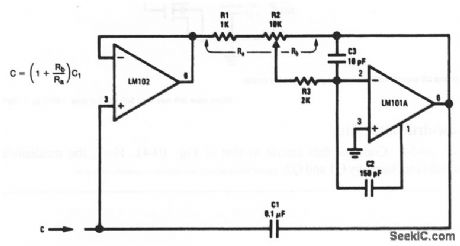
This circuit appears as an adjustable capacitance (set by R2) to the input. (View)
View full Circuit Diagram | Comments | Reading(673)
Negative_ca_pacitancem_ultiplier
Published:2009/7/23 22:37:00 Author:Jessie
This circuit appears as a negative capacitance to the input. (View)
View full Circuit Diagram | Comments | Reading(651)
160_W_PEP_broadband_linear_amplifier
Published:2009/7/23 22:54:00 Author:Jessie
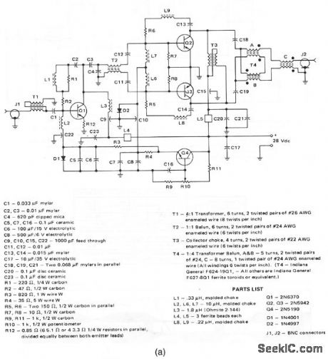
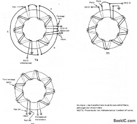
This circuit provides 160-W (PEP) into a 50-Ω load with an IMD (intermodulation distortion) of -30 dB Or better,Figure 2-50B shows the transformer details. (View)
View full Circuit Diagram | Comments | Reading(0)
25_W_UHF_amplifier_using_microstrip_techniques
Published:2009/7/23 22:52:00 Author:Jessie
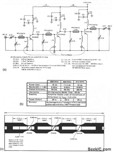
This circuit provides 25-W of output power in the 450- to 512-MHz UHF band, and is designed for 12.5-V operation. Figure 2-49B shows typical amplifier performance data. Figure 2-49C shows the microstrip board layout.Those not familiar with microstrip techniques should read the many Motorola publications, such as AN548A and AN555. (View)
View full Circuit Diagram | Comments | Reading(801)
| Pages:124/250 At 20121122123124125126127128129130131132133134135136137138139140Under 20 |
Circuit Categories
power supply circuit
Amplifier Circuit
Basic Circuit
LED and Light Circuit
Sensor Circuit
Signal Processing
Electrical Equipment Circuit
Control Circuit
Remote Control Circuit
A/D-D/A Converter Circuit
Audio Circuit
Measuring and Test Circuit
Communication Circuit
Computer-Related Circuit
555 Circuit
Automotive Circuit
Repairing Circuit