
Amplifier Circuit
Index 128
Compandor_with_90_dB_dynamic_range
Published:2009/7/24 0:03:00 Author:Jessie
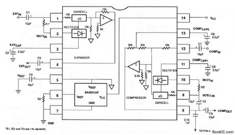
This NE/SA577 circuit is similar to that of Fig. 1-34, except that there is no power-down/mute function, and there is no summing input to the compressor. (View)
View full Circuit Diagram | Comments | Reading(748)
Compandor_with_80_dB_dynamic_range_and_power_down_mute
Published:2009/7/24 0:02:00 Author:Jessie
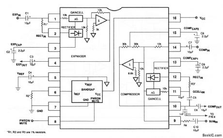
This single-chip NE/SA576 circuit operates on voltages from 1.8 V to 7 V, with a power consumption of 1.4 mA at 3.6V. Multiple external signals can be summed in the compandor at pin 9. The gain level can be programmed by the selection of resistors R1, R2, and R3. If the supply is less than 2 V, connect 20-kΩ resistors between Vcc and VREF, and between VREF and ground (so that the IC will turn on with a 1.8-V supply). The power-down/mute function (pin 8) requires an open-collector signal, and is active-low. (View)
View full Circuit Diagram | Comments | Reading(901)
Single_chip_audio_amplifier_BTL_stereo_1_W
Published:2009/7/23 23:58:00 Author:Jessie
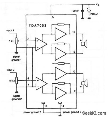
This circuit is similar to that of Fig. 1-27, except that no built-in volume control is provided, and two (stereo) channels are available. The supply range is from 3 V to 18 V. The circuit provides a 1-W per channel output, with a 6-V supply, into 8-Ω stereo loads, or 2-W per channel output, with an 11-V supply, into 25-Ω loads. Fixed, closed-loop voltage gain is 39 dB (6-V supply, 8-Ω load). (View)
View full Circuit Diagram | Comments | Reading(990)
Smgle_chip_audio_amplifier_BTL_mono_1_W_2_W
Published:2009/7/23 23:57:00 Author:Jessie
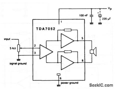
This circuit is similar to that of Fig. 1-27, except that no built-in volume control is provided. The supply range is from 3 V to 18 V. The circuit provides an output of 1W, with a 6-V supply, into an 8-Ω load, or 2-W output when the supply is raised to 11 V, into a 25-Ω load. Fixed, closed-loop voltage gain is 39 dB (6-V supply, 8-Ω load). (View)
View full Circuit Diagram | Comments | Reading(789)
Single_chiyo_audio_amplifier_BTL_1_W_05_W_with_volume_control
Published:2009/7/23 23:56:00 Author:Jessie
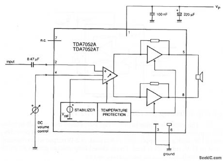
This circuit makes use or the bridge-tied load (BTL) principle to achieve low-voltage operation without sacrifice of output power. The wide supply range (4.5 V to 18 V) makes the circuit suitable for a broad range of applications (battery-powered radios, telephone sets, etc.). The IC amplifier has a built-in dc volume control, with a log characteristic range of more than 80 dB.When the dc control voltage (pin 4) drops below 0.3 V, the amplifier is muted, so there are no switch-on/switch -off clicks. The TDA7052A provides an output of 1 W with a 6-V supply into an 8-Ω load, or 2-W output when the supply is raised to 12 V, into a 32-Ω load. The TDA7052AT output is 0.5 W with a 6-V supply, into a 16-Ω load. Basic amplifier circuit titles and descriptions (View)
View full Circuit Diagram | Comments | Reading(756)
ELECTROMYOGRAM_AMPLIFIER
Published:2009/7/3 2:09:00 Author:May
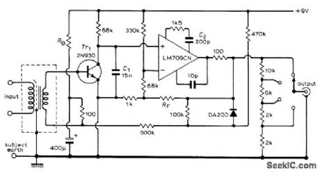
Used to amplify voltages in range of several microvolts to several millivolts in frequency spectrum of 20 to 5000 Hz, as picked up with 13-mm thin silver disks placed on skin over muscle being studied.Article also covers electrocardiographin applications involving source impedances as high as 50 kilohms (as with one electrode on each wrist). Maximum output capability is 9 V P-P.Voltage gain is 1000. RF is 800K pot, ad lusted to give 12 dB per octave dropoff above turnover frequency.-R. E. George, Simple Amplifier for Muscle Voltages, Wireless World, Oct. 1972, p 495-496. (View)
View full Circuit Diagram | Comments | Reading(1237)
Compandor_with_90_dB_range_and_power_down_mute
Published:2009/7/24 0:04:00 Author:Jessie
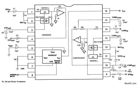
This NE/SA578 circuit is similar to that of Fig.1-34,except that the programmable dynamic range is 90 dB. (View)
View full Circuit Diagram | Comments | Reading(598)
DIRECT_COUPLED_AMPLIFIER
Published:2009/7/24 1:46:00 Author:Jessie
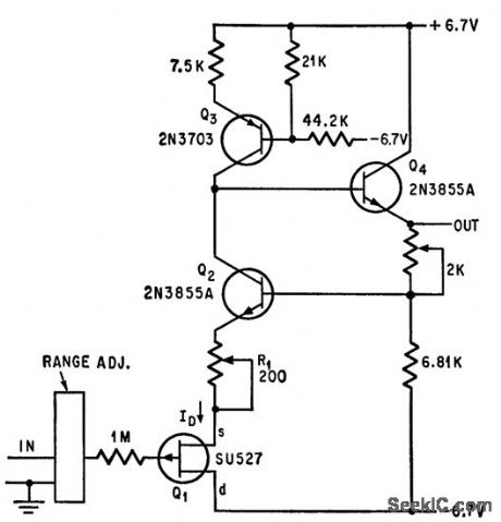
Gives high input impedance and low drift at low cost, with approximately unity gain. Uses one fet and three bipolar transistors. Suitable for d-c voltmeter having 0.1 v full scale on lowest range. Temperature drift is low.-J. M. Colwell, Direct-Coupled Amplifier Cuts Cost of D-C Voltmeter, Electronics, 39:12, p 109-110. (View)
View full Circuit Diagram | Comments | Reading(1578)
Single_chip_log_amplifier_75_dB
Published:2009/7/24 0:13:00 Author:Jessie
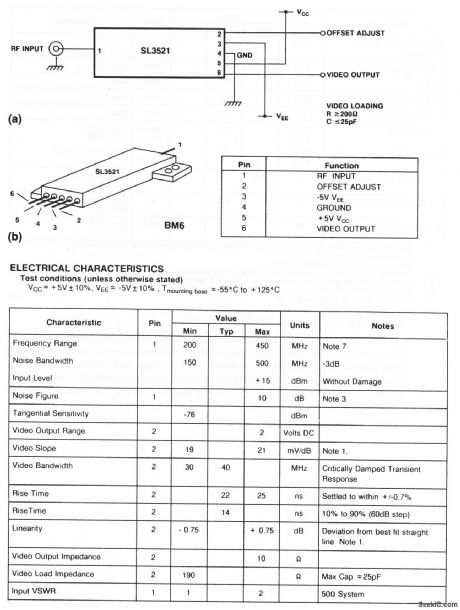
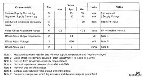
The SL3521 used in this circuit is a successive-detection log amp IC for use in the 100- to 650-MHz range. The IC provides a video output with offset adjust. Figure 2-3B shows the pin connections. Figure 2-3C shows the electrical characteristics. The offset voltage at pin 2 should be in the -0.45- to -0.55-V range, and must not be such as to increase the output offset to more than±0.5 V (View)
View full Circuit Diagram | Comments | Reading(859)
IMPLANT_AMPLIFIER
Published:2009/7/3 1:39:00 Author:May
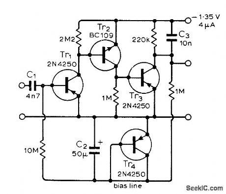
Designed for use in implanted transmitters monitoring brain and heart potentials. Requires only 4μA at 1.35 V.Voltage gain is 2000, and equivalent input noise only 10 μV P-P with 10-megohm source impedance. Tr1 is current-starved, but resulting limited bandwidth of about 5 kHz is acceptable for biological applications.-C. Horwitz, Micropower Low-Noise Amplifier, Wireless World, Dee. 1974, p 504. (View)
View full Circuit Diagram | Comments | Reading(729)
Single_chip_log_limiting_amplifier_75_dB
Published:2009/7/24 0:11:00 Author:Jessie
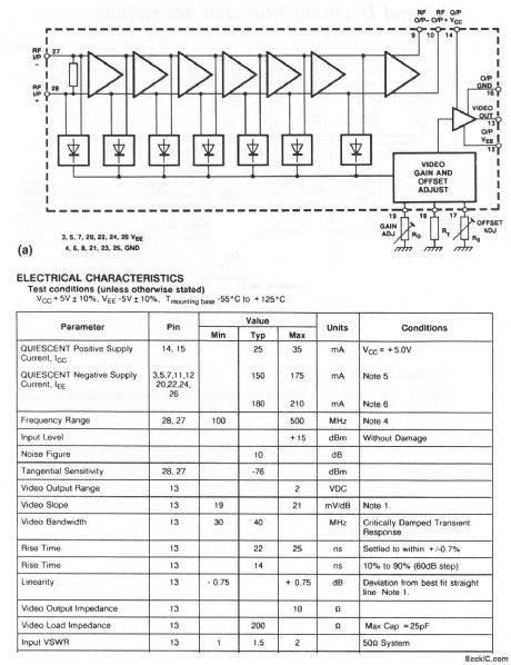
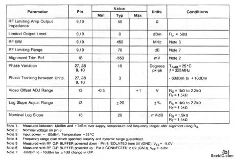
The SL3522 used in this circuit is a 7-stage successive-detection log amp IC for use in the 100- to 600-MHz range. The IC features an on-chip video amplifier with provision for extemal adjustment of log slope and offset, as well as a balanced RF output. Figure 2-2B shows the electrical characteristics. Compare this single-chip circuit to that of the multi-chip amplifier in Fig. 2-1. (View)
View full Circuit Diagram | Comments | Reading(738)
2_METER_IC_RF_AMPLIFIER_
Published:2009/7/2 23:37:00 Author:May
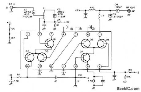
High-gain double compound amplifier using RCA CA3102E haslow noise、 excelle tstabity、 and only twotuned circuits,Ideal for 2-meter FM RF stage,but can be used from DC up to 500 MHz by changing tuned circuits Article covers construction、with emphasis on proper shielding.-B.Hoisington,Two High Gain RF Stages One IC for Two Meter FM 73 Magaze,May 1974,p 47-50 and 52. (View)
View full Circuit Diagram | Comments | Reading(1010)
SUMMING_AMPLIFlER
Published:2009/7/2 23:25:00 Author:May
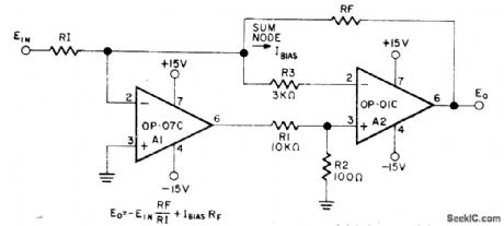
Combination of Precision Monolithics OP-07C and OP-01C opamps gives 18 V/μs slew rate. Can be used as current.output summing amplifier for D/A converter because it requires no zero scale offset adjustments and high speed is preserved.-D. Soderquist and G. Erdi. The OP-07 Ultra-Low Offset Voltage Op Amp-a Bipolar Op Amp That Challenges Choppers. Eliminates Nulling. Precision Monolithics. Santa Clara. CA. 1975. AN-13. p 9. (View)
View full Circuit Diagram | Comments | Reading(871)
UNITY_GAIN_FEED_FORWARD
Published:2009/7/2 23:17:00 Author:May
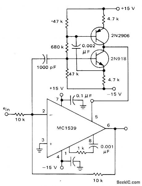
Provides 10 V P-P output signal at 2 MHz when gain of feedforward amplifier is increased to give closedloop gain of 10. Provides fast response to stepfunction input. with slow settling. High-frequency circuit takes over completely when input frequency is too high for input stage to respond.-E. Renschler. The MC1539 Operational Amplifier and Its Applications. Motorola. Phoenix. AZ. 1974. AN-439. p 20. (View)
View full Circuit Diagram | Comments | Reading(842)
Ultra_low_noise_wideband_preamplifier
Published:2009/7/24 0:25:00 Author:Jessie
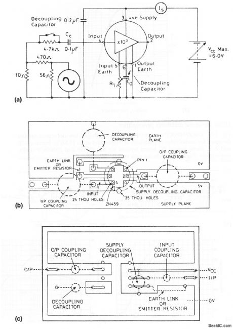
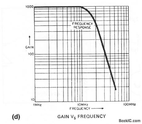
The ZN459/CP used in this circuit is a high-gain low-noise preamplifier designed for audio/video applications at frequencies up to 15MHz. Figures 2-7B and 2-7C show typical PC board layouts for the ZN459 and ZN459CP (DIP), respectively .Figure 2-7D shows gain versus frequcncy. (View)
View full Circuit Diagram | Comments | Reading(1005)
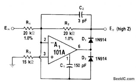
ABSOLUTE_VALUE_AMPLIFIER
Published:2009/7/2 21:49:00 Author:May
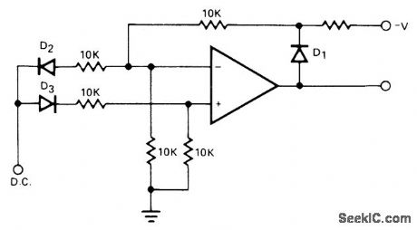
Generates positive output voltage for either polarity of DC input. Opamp and diode types are not critical. Accuracy is highest for input voltages greater than 1 V. Opamp is noninverting on positive signals and inverting on negative signals.- Signetics Analog Data Manual. Signetics, Sunnyvale. CA. 1977. p 641-643. (View)
View full Circuit Diagram | Comments | Reading(0)
3_W_POWER_AMPLIFIER_FOR_SPLIT_PHASE_MOTOR
Published:2009/7/24 1:29:00 Author:Jessie
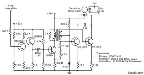
Capacitor tunes motor to make load more resistive. Feedback is used to lower output impedance and thereby improve transient response of motor. Used in digital servo system.-Texas Instruments Inc., Transistor Circuit Design, McGraw-Hill, N.Y., 1963, p 493. (View)
View full Circuit Diagram | Comments | Reading(725)
SUMMING_AMPLIFIER
Published:2009/7/2 21:18:00 Author:May
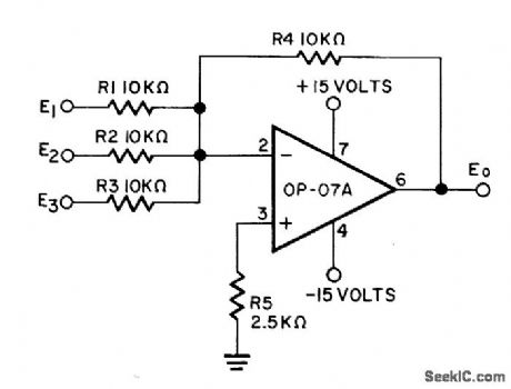
Provides output equal to sum of all input voltages. with high precision. Use of Precision Monolithics OP-07A opamp makes circuit adiustment-free.- Ultra-Low Offset Voltage Op Amp. Precision Monolithics. Santa Clara. CA. 1977. OP-07. p 7. (View)
View full Circuit Diagram | Comments | Reading(0)
ERROR_RATE_COMPENSATION_AMPLIFIER
Published:2009/7/24 1:39:00 Author:Jessie
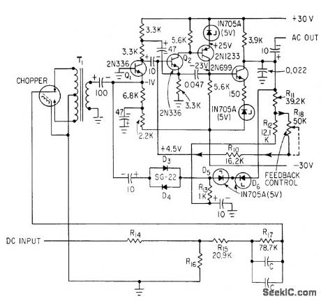
Chopped d-c input is fed to Q2 through T1 and Q1. Base of Q2 is amplifier summing point and receives feedback signals. Gain is 2.73 V rms per volt d-c.-E. R. Schlesinger, Aiming a 3-Ton Telescope Hanging from Balloon, Electronics, 36:6, p 47-51. (View)
View full Circuit Diagram | Comments | Reading(559)
450_MHz_high_gain_amplifier_6_V_supply
Published:2009/7/24 2:28:00 Author:Jessie

The electrical characteristics for the 2N5031/32 shown in this circuit are given in Fig. 2-19B. (View)
View full Circuit Diagram | Comments | Reading(554)
| Pages:128/250 At 20121122123124125126127128129130131132133134135136137138139140Under 20 |
Circuit Categories
power supply circuit
Amplifier Circuit
Basic Circuit
LED and Light Circuit
Sensor Circuit
Signal Processing
Electrical Equipment Circuit
Control Circuit
Remote Control Circuit
A/D-D/A Converter Circuit
Audio Circuit
Measuring and Test Circuit
Communication Circuit
Computer-Related Circuit
555 Circuit
Automotive Circuit
Repairing Circuit