
Amplifier Circuit
Index 125
Linear_amplifier_using_wideband_hybrids
Published:2009/7/23 22:50:00 Author:Jessie
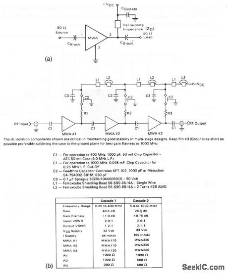
This circuit shows three wideband hybrid amplifiers cascaded to form a linear amplifier. Figure 2-48B shows the hybrid amplifier connections. As shown by the table, the circuit is capable of operation from 0.25 to 400 MHz (or 5 to 1000 MHz), depending on the selection of components and power sources. (View)
View full Circuit Diagram | Comments | Reading(713)
Thermally_controlled_NiCad_battery_charger
Published:2009/7/23 22:43:00 Author:Jessie
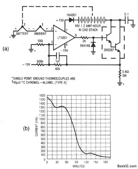
This circuituses an LT1001 and a2N3687 Darlington to form a simple charger for NiCad batteries. The batteries can be charged at a high rate without danger because the cell temperature is measured, and the charging rate is adjusted accordingly. Notice that two thermocouples are used. The battery thermocouple is mounted on one of the cells in the pack, and the ambient thermocouple is exposed to ambient temperature (mounted on a thermal mass that approximates that of the battery pack). The thermocouple voltages cancel and the positive input of the LT1001 is at zero. the temperature difference between the two thermocouples determines the input. As battery temperature rises, this small negative voltage (1°C difference between thermocouples equals 40 μV) becomes larger. The LT1001, operating at a gain of 4300, gradually reduces current through the battery to maintain a balance at the LT1001 input. The effect of this action is shown in Fig. 10-60B. The battery charges at a high rate until heating occurs and the circuit then tapers the charge. With the values shown, the battery-surface temperature rise (above ambient) is limited to the very safe level of 5°C. (View)
View full Circuit Diagram | Comments | Reading(665)
Amplifier_with_10_dB_gain_over_nine_octaves
Published:2009/7/23 23:16:00 Author:Jessie

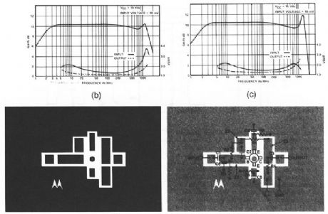
This circuit has a gain of about 10 dB from 3 MHz to over 1GHz (Fig.2-59B). The gain/VSWR versus frequency, PC-board photomaster, and parts layout are shown in Figs. 2-59C, 2-59D, and 2-59E, respectively. The actual layout dimensions are: 1.8 x 1.2 . Two type OSM215 50-Ω input and output connectors can be mounted opposite to the component side of the board, if required. (View)
View full Circuit Diagram | Comments | Reading(1006)
Precision_instrumentation_amplifier
Published:2009/7/23 23:16:00 Author:Jessie
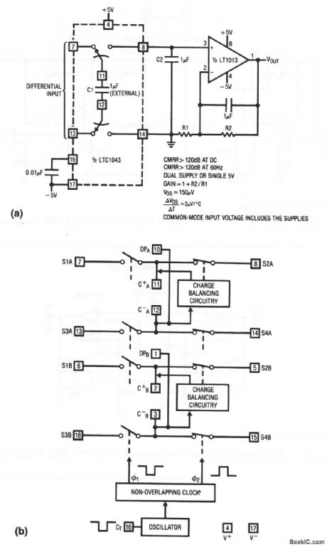
This circuit uses an LTC1043 switched-capacitor IC (Fig. 1-4B) and an LT1013 op amp to form a simple, precise instrumentation amplifier. The 0.01-μF capacitor at pin 16 sets the switching frequency at 500 Hz. (View)
View full Circuit Diagram | Comments | Reading(903)
RIAA_preamplifier
Published:2009/7/23 23:15:00 Author:Jessie
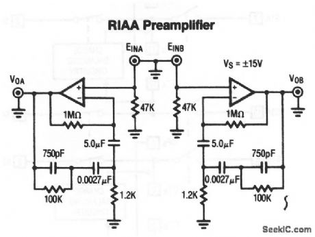
This circuit also uses both halves of an RC4995 (Fig .5-11B) (View)
View full Circuit Diagram | Comments | Reading(0)
40__to_900_MHz_broadband_amplifier
Published:2009/7/23 23:14:00 Author:Jessie
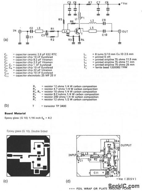
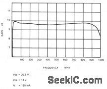
This circuit has a gain of about 9.5 dB over the frequency range, and delivers an output of about 1.2 V into 75Ω, with an IMD level of about -60 dB.The components lists, PC-board photomaster, components layout, and gain are shown in Figs. 2-58B, 2-58C, 2-58D, and 2-58E, respectively. (View)
View full Circuit Diagram | Comments | Reading(743)
10_W_CLASS_B_SERVO_AMPLIFIER
Published:2009/7/23 23:32:00 Author:Jessie
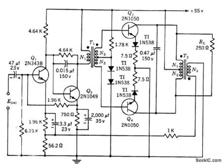
Gives power gain of 39 db. Voltage amplification is constant within 1 db of 32.5 db. Transformer data is for 400-cps operation. -Texas Instruments Inc., Transistor Circuit Design, McGraw-Hill, N.Y., 1963, p 243. (View)
View full Circuit Diagram | Comments | Reading(788)
5_W_400_MHz_TM0S_FET_amplifier
Published:2009/7/23 23:01:00 Author:Jessie
This circuit uses an MRF134 and has a gain of 10.5 dB. (View)
View full Circuit Diagram | Comments | Reading(643)
5_W_150_MHz_TMOS_FET_amplifier
Published:2009/7/23 23:00:00 Author:Jessie

This circuit uses an MRF134, has a gain of 14dB, and has a drain efficiency of 55%. The output amplitude can be adjusted by R3. (View)
View full Circuit Diagram | Comments | Reading(549)
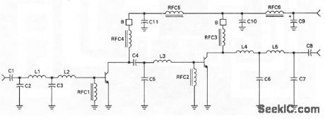
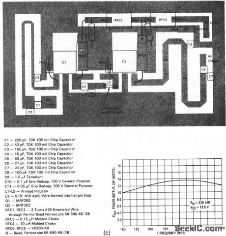
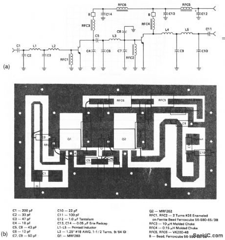
30_W_150__to_175_MHz_amplifier
Published:2009/7/23 23:08:00 Author:Jessie
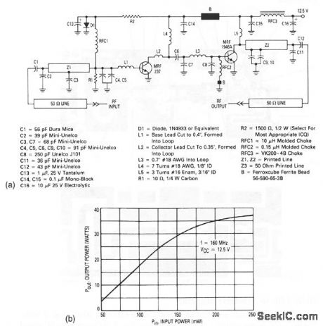
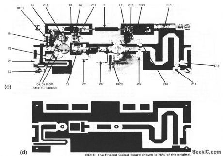
This circuit produces an overall gain in excess of20 dB (Fig. 2-56B).Figure 2-56C shows typical parts placement, and Fig. 2-56D shows the PC-board photomaster (actual dimensions: 5 x 2 ). The amplifier is constructed on 1/16 , double-sided G-10 board with 2-ounce copper cladding. The top and bottom ground planes of the board are connected by wrapping the board edges with thin copper foil (0.002 ) and then soldering the foil in place. The MRF237 is inserted into a hole in the board and soldered to the ground plane for heatsinking. The MRF1946A is mounted on a conventional heatsink (an 8-32 stud inserted into an appropriately prepared heatsink). Refer to Motorola AN778 and AN790 for mounting and thermal ratings of power transistors.
(View)
View full Circuit Diagram | Comments | Reading(2066)
Stereo_tone_control
Published:2009/7/23 23:13:00 Author:Jessie
This circuit uses both halves of an RC4559 (Fig. 5-11B) (View)
View full Circuit Diagram | Comments | Reading(2121)
300_W_FM_88__to_108_MHz_power_amplifier
Published:2009/7/23 23:11:00 Author:Jessie

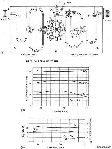


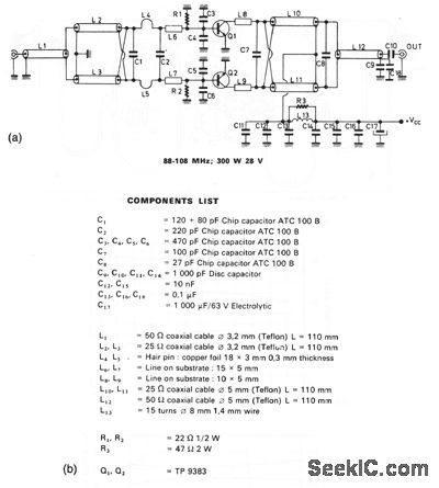

This circuit has a galn of about 9 dB over the frequency range.Thecomponents list,component layout,output power Versus input power and frequency, and gain are shown in Figs. 2-57B, 2-57C, 2-57D, and 2-57E, respectively. The actual layout dimensions are: 4.25 × 2.25 . (View)
View full Circuit Diagram | Comments | Reading(886)
Low_impedance_microphone_preamplifier
Published:2009/7/23 23:10:00 Author:Jessie
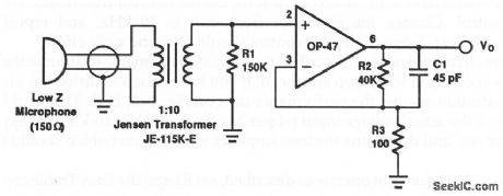
In this preamp, the transformer converts the low microphone impedance up to a value (about 7 kΩ) required by the OP-47 for best noise performance.C1 rolls off the high-frequency response at 90 kHz, giving a noise power bandwidth of 140 kHz. (View)
View full Circuit Diagram | Comments | Reading(1739)
Single_chip_audio_amplifier_stereo_2_×0075W
Published:2009/7/23 23:54:00 Author:Jessie
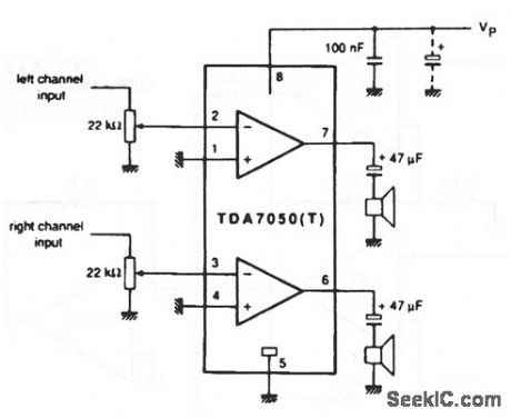
This low-voltage amplifier is for stereo applications (small speaker or headphones ).The circuit operates with battery supplies, from 6V down to 1.6V,and draws low quiescent current (typically 3.2mA with 3-V supply),Closed-loop voltage gain is 26dB with connections as shown, Output is 2×0.075W,with a 4.5-V supply ,operating 32-Ω loads ,The output is reduced to 2×0.035W when the supply is reduced to 3V (with 32-Ωloads). (View)
View full Circuit Diagram | Comments | Reading(758)
Low_noise_technique_with_parallel_amplifiers
Published:2009/7/23 23:53:00 Author:Jessie
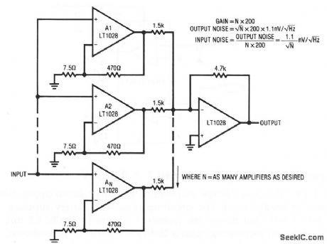
This circuit operates on a statistical noise-reduction technique. Noise decreases by the √N of the number of devices in parallel. For example, for nine paralleled amplifiers, noise would decrease by a factor of three, to about 0.33 nV √Hz at 1 kHz. A potential penalty of this connection is that the input-current noise increases by √N devices. (View)
View full Circuit Diagram | Comments | Reading(1069)
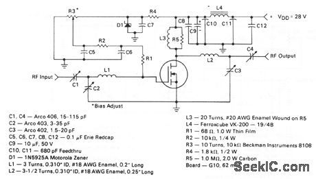
Low_cost_VHF_broadband_amplifier_160_to_174_MHz
Published:2009/7/23 23:24:00 Author:Jessie
This circuit has a power gain of about 18 dB overthe frequency range.Figure 2-62B shows the board layout and components list, and Fig,2-62C showsthe power output Versus frequency. (View)
View full Circuit Diagram | Comments | Reading(1315)
Amplifier_with_CMOS_inverter_output_stage
Published:2009/7/23 23:24:00 Author:Jessie
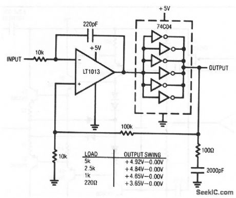
This circuit shows a simple, inexpensive way to extend the output swing of an amplifier to the supply rails. The circuit is particularly useful in 5-V analog systems, where improvements in available output swing are desirable to maximize signal-processing range. As shown by the table, output swing is quite close to the positive rail, particularly at loads below several mA. (View)
View full Circuit Diagram | Comments | Reading(858)
Ultra_frtst_amplifier_with_current_boost
Published:2009/7/23 23:23:00 Author:Jessie
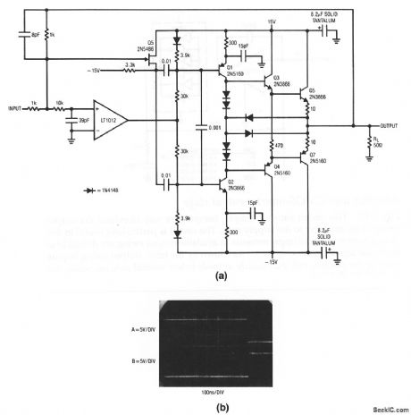
This current-boosted amplifier features a slew rate in excess of 1000 V/μs, a full power bandwidth of 7.5 MHz, and a 3-dB point of 14 MHz. Figure 1-9B shows the circuit driving a 10-V pulse into a 50-Ω load. Trace A is input, Trace B is output. (View)
View full Circuit Diagram | Comments | Reading(893)
Low_cost_VHF_broadband_amplifier_136_to_160_MHz
Published:2009/7/23 23:23:00 Author:Jessie
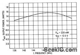
This circuit has a power gain of about 19 dB over the frequency range.Figure 2-61B shows the board layout and components list, and Fig. 2-61C shows the power output versus frequency. (View)
View full Circuit Diagram | Comments | Reading(1543)
Lock_in_amplifier
Published:2009/7/23 23:19:00 Author:Jessie
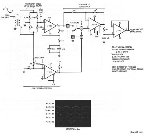
carrier-modulated output of the signal source. Because the desired signal information is contained within the carrier, the system constitutes an extremely narrowband amplifier. Noncarrier related components are rejected, and the amplifier passes only signals, which are coherent with the carrier. The amplifier can extract a signal 120 dB below the noise level. The signal source is a thermistor bridge, which detects extremely small temperature shifts in a biochemical microcalorimetry reaction chamber. To trim, adjust the phase potentiometer so that switching occurs when the carrier crosses through zero. (View)
View full Circuit Diagram | Comments | Reading(1954)
| Pages:125/250 At 20121122123124125126127128129130131132133134135136137138139140Under 20 |
Circuit Categories
power supply circuit
Amplifier Circuit
Basic Circuit
LED and Light Circuit
Sensor Circuit
Signal Processing
Electrical Equipment Circuit
Control Circuit
Remote Control Circuit
A/D-D/A Converter Circuit
Audio Circuit
Measuring and Test Circuit
Communication Circuit
Computer-Related Circuit
555 Circuit
Automotive Circuit
Repairing Circuit