
Amplifier Circuit
Index 136
Trigger_with_adaptive_threshold
Published:2009/7/24 7:33:00 Author:Jessie
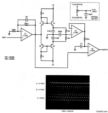
This circuit triggers from dc to 50 MHz over a 2- to 300-mV input range with no level adjustment. The circuit maintains the A3 output trip-point at one-half the input amplitude, regardless of input magnitude. This ensures reliable automatic triggering over a wide input amplitude range-even for very low-level inputs. As an option, the network shown in dashed lines permits changing the trip threshold. This allows any point on the input waveform edge to be selected as the trigger point. Figure 5-22B shows performance for a 40-MHz input sine wave (Trace A). The A1 output (Trace B) takes gain and the A3 output (Trace C) produces a clean 5-V signal. Linear Technology Corporation, 1991, AN47-59. (View)
View full Circuit Diagram | Comments | Reading(930)
AGC_AMPLIFIER
Published:2009/6/30 22:24:00 Author:May
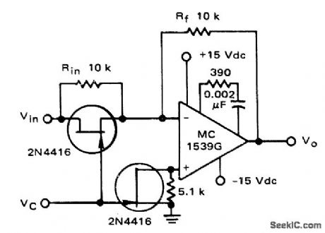
FET used in conjunction with opamp permits varying of gain by changing ratio of Rf to Rin. Offset voltage in output due to input bias currents is minimized by placing FET in parallel with 5.1K resistor between noninverting leg of opamp and ground, so resistance varies with changes of It,,- Low Frequency Applications of Field-Effect Transistors, Motorola, Phoenix, AZ, 1976, AN-511A, p 9. (View)
View full Circuit Diagram | Comments | Reading(2203)
WIDEBAND_AGC_AMPLIFIER
Published:2009/6/30 22:23:00 Author:May
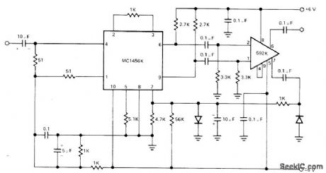
Combination of 592K opamp and MC1496K balanced modulator gives DC output signal proportional to amplitude of AC input signal, for varying gain of balanced modulator. Unbalancing carrier input of modulator makes signal pass through without attenuation.- Sig netics Analog Data Man-ual, Signetics, Sunnyvale, CA, 1977, p 709-710. (View)
View full Circuit Diagram | Comments | Reading(1395)
HIGH_SPEED_SAMPLE_AND_HOLD_AMPLIFIER
Published:2009/6/30 3:29:00 Author:May
View full Circuit Diagram | Comments | Reading(622)
AUDIO_AGC_USING_FET
Published:2009/6/30 22:21:00 Author:May
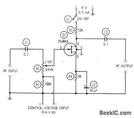
DC control voltage obtained from key signal point in audio amplifer is applied to gate of FET to vary bias. Gain of stage varies inversely with gate bias voltage.When control voltage is 0 V, voltage gain of stage is to and maximum undistorted output signal is 1 VRMS. When control voltage is 6 VDC, output is reduced to 0.5 mVRMS, giving better than 90-dB range for AGC controL-R. P.Tuner, FET Circuits, Howard W. Sams, Indi-anapolis, IN 1977, 2nd Ed., p 39-40. (View)
View full Circuit Diagram | Comments | Reading(1669)
50_54_MHz_RF_AGC_AMPLIFIER
Published:2009/6/30 22:20:00 Author:May
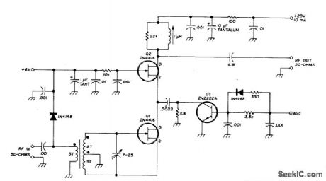
Developed for 6-roeter SSB transceiver to give minimum of 15-dB power gain, low noise figure, and good signal-handling capability when AGC is applied.AGC control resembles bipolar cascode drcuit using differential pair with current source, although operation does not involve changing amplifier bias Ievel. With increasing AGC voltage, a3 begins to turn on, shunting more and more signal cument away from 02 and thereby decreasing stage gain. Input transformer is wound on small toroid core. Range of AGO volt-age is 0-1.2 V.-A. Borsa, High-Performance BF-AGC Amplifier, Ham Radio, Sept. 1978, p 64-66. (View)
View full Circuit Diagram | Comments | Reading(2403)
IF_AMPLIFIER
Published:2009/6/30 21:22:00 Author:May
View full Circuit Diagram | Comments | Reading(1801)
TV_SOUND_IF_OR_FM_IF_AMPLIFIER_WITH_QUADRATURE_DETECTOR
Published:2009/6/30 21:18:00 Author:May
View full Circuit Diagram | Comments | Reading(1596)
TWO_STAGE_WIDEBAND_AMPLIFIER
Published:2009/6/30 21:15:00 Author:May
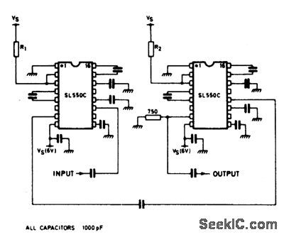
A wideband high gain configuration using two SL550s connected in series. The first stage is connected in common emitter config-uration, the second stage is a common base circuit. Stable gains of up to 65 dB can be achieved by the proper choice of R1 and R2. The bandwidth is 5 to 130 MHz, with a noise figure only marginally greater than the 2.0 dB specified for a single stage circuit. (View)
View full Circuit Diagram | Comments | Reading(752)
TELEVISION_IF_AMPLIFIER_AND_DETECTOR_USING_AN_MC1330_AND_AN_MC1352
Published:2009/6/30 21:14:00 Author:May
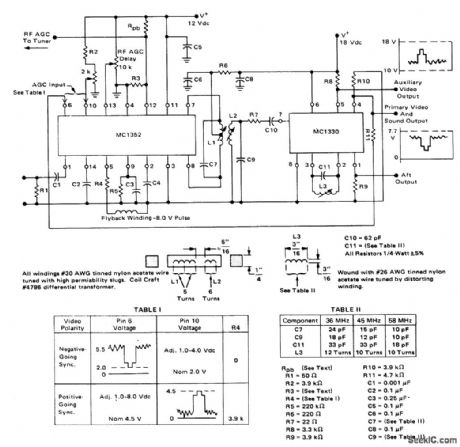
View full Circuit Diagram | Comments | Reading(988)
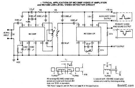
VIDEO_IF_AMPLIFIER_AND_LOW_LEVEL_VIDEO_DETECTOR_CIRCUIT
Published:2009/6/30 21:13:00 Author:May
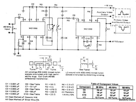
The circuit has a typical voltage gain of 84 dB and a typical AGC range of 80 dB. It gives very small changes in bandpass shape, usually less than 1 dB tilt for 60 dB compression. There are no shielded sections. The detector uses a single tuned circuit (L3 and C10). Cou-pling between the two integrated circuits is achieved by a double tuned transformer (L1 and L2). (View)
View full Circuit Diagram | Comments | Reading(1220)
HIGH_SPEED_SAMPLE_AND_HOLD_1
Published:2009/6/30 3:33:00 Author:May
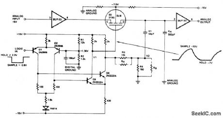
This circuit exhibits a 10 V acquisition time of 900 ns to 0.1% accuracy and a droop rate of only 100 μV/ms at 25°C ambient condition. An even faster acquisition time can be obtained using a smaller value hold-capacitor. By decreasing the value from 1000 pF to 220 pF, the acquisition time improves to 500 ns for a 10 V step. However, the droop rate increases to 500 μV/ms. (View)
View full Circuit Diagram | Comments | Reading(1014)
TEMPERATURE_COMPENSATION
Published:2009/6/30 3:06:00 Author:May
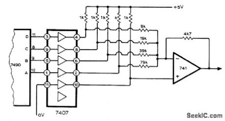
Use of 7407 hex buffer following SN7490 of D/A converter permits satisfactory performance over reasonably wide temperature range even when driving several TTL stages. Noninverting input of 741 opamp is connected to output of unused buffer at logic 0. Circuit is modification of D/A converter developed by D. James for use in simple two-digit DVM.—R. J. Chance, Improved Simple D. to A. Convener, Wireless World, Dec, 1974.p 503. (View)
View full Circuit Diagram | Comments | Reading(1256)
Bilateral_current_source_with_balance
Published:2009/7/24 21:39:00 Author:Jessie
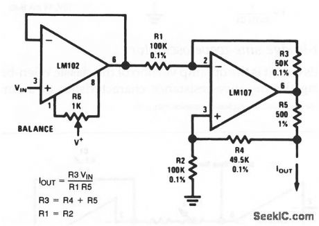
The current output of this circuit depends on the input voltage and the resistance ratios, as shown by the equations. Current output can be trimmed by R6. (View)
View full Circuit Diagram | Comments | Reading(896)
Double_ended_limit_detector
Published:2009/7/24 21:26:00 Author:Jessie
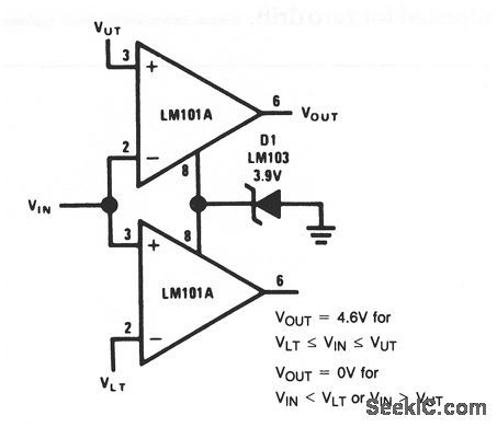
This circuit compares the input voltage with an upper and lower voltage limit. (View)
View full Circuit Diagram | Comments | Reading(2408)
HIGH_SPEED_OUTPUT_OPAMP
Published:2009/6/30 2:55:00 Author:May
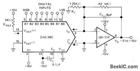
Precision Monolithics OP-17F opamp optimizes DAC-08E D/A converter for highest speed in converting DAC output current to output voltage up to lO V under control of digital input. Settling time is 380 ns.—G. Erdi, The OP-17, OP-16, OP-15 as Output Amplifiers for High Speed D/A Converters, Precision Monolithics, Santa Clara, CA, 1977, AN-24, p 2. (View)
View full Circuit Diagram | Comments | Reading(611)
Low_pass_active_filter_with_Norton_amplifier
Published:2009/7/24 13:34:00 Author:Jessie
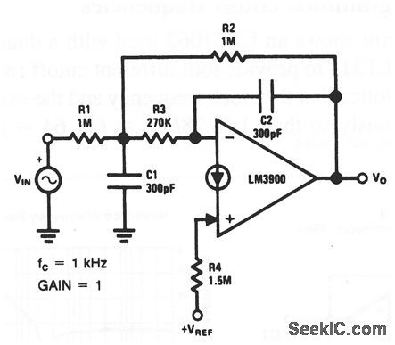
This circuit uses an LM3900 Norton amplifier as a 1-kHz low-pass filter. National Semiconductor, Linear Applications Handbook, 1991, p. 227. (View)
View full Circuit Diagram | Comments | Reading(1037)
High_pass_active_filter_with_Norton_amplifier
Published:2009/7/24 13:33:00 Author:Jessie
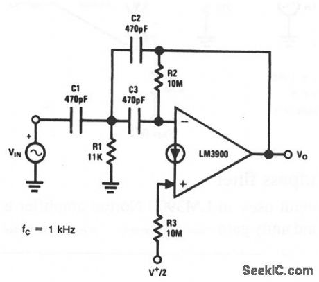
This circuit uses an LM3900 Norton amplifier as a 1-kHz high-pass filter. National Semiconductor, Linear Applications Handbook, 1991, p. 227. (View)
View full Circuit Diagram | Comments | Reading(767)
SQUELCHABLE_AMPLIFIER
Published:2009/6/30 2:05:00 Author:May
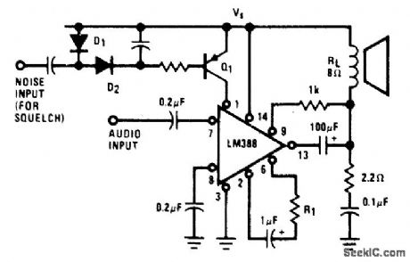
Circuit designed for portable FM scanners and two-way walkietalkie radios can be tumed off by noise or by control signal to minimize battery drain. When squelched, LM388 opamp-transistor-diode anay draws only 0.8 mA from 7.5-V supply.Diodes rectify noise from Iimiter or discriminator of receiver, producing direct current that tums on Q1 and thereby clamps opamp off. Voltage gain is 20 to 200, depending on value used for R1. Power output without squelch is about 0.5 W for 8-ohm loudspeaker.- Audio Hand-book. National Semiconductor, Santa Clara, CA, 1977, p 4.37-4-41. (View)
View full Circuit Diagram | Comments | Reading(3551)
FILTERED_BUFFER
Published:2009/6/30 1:55:00 Author:May
Used with Motorola MC1505 AiD converter when making precise measurements of slowly varying DC voltages in digital voltmeters or in feedback controls.Closed-loop front-end buffer provides high input impedance and reduces stray noise and 60-Hz pickup. Two-pole filter is included in unity-feedback loop of buffer. Front-end scaling circuit is induded with buffer.—D. Aldridge and S. Kelley, Input Buffer Circuits for the MC1505 Dual Ramp A-to-D Converter Subsystem, Motorola, Phoenix, AZ, 1976, EB-24A. (View)
View full Circuit Diagram | Comments | Reading(1036)
| Pages:136/250 At 20121122123124125126127128129130131132133134135136137138139140Under 20 |
Circuit Categories
power supply circuit
Amplifier Circuit
Basic Circuit
LED and Light Circuit
Sensor Circuit
Signal Processing
Electrical Equipment Circuit
Control Circuit
Remote Control Circuit
A/D-D/A Converter Circuit
Audio Circuit
Measuring and Test Circuit
Communication Circuit
Computer-Related Circuit
555 Circuit
Automotive Circuit
Repairing Circuit