
Amplifier Circuit
Index 103
6_W_AUDIO_AMPLIFIER_WITH_PREAMP
Published:2009/7/9 2:12:00 Author:May

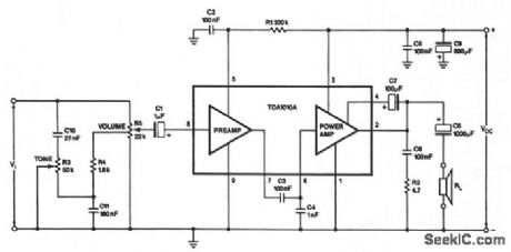
This monolithic IC, class-B, audio amplifter circuit is a 6-W car radio amplifter for use with 4-Ω and 2- Ω load impedances. (View)
View full Circuit Diagram | Comments | Reading(879)
AUDIO_POWER_AMPLIFIER
Published:2009/7/9 2:08:00 Author:May
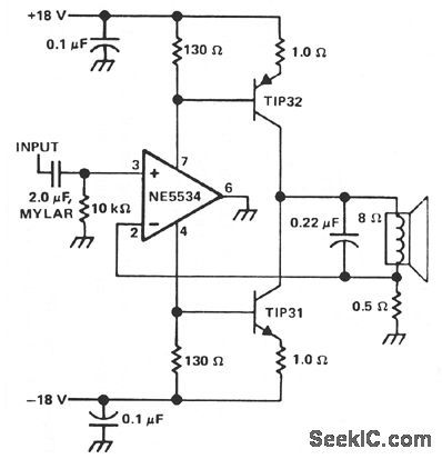
he single speaker amplifier circuit uses cur-rent feedback, rather than the more popular voltage feedback. The feedback loop is from the junction of the speaker terminal and a 0.5-Ω resistor, to the inverting input of the NE5534. When the input to the amplifier is positive, the power supply supplies current through the TIP32 and the load to ground.Conversely, with a negative input, the TIP31 sup-plies current through the load to ground. The gain is set to about 15 (gain SPKR 8 Ω/0.5 Ω feed-back). The 0.22-μF capacitor across the speaker rolls off its response beyond the frequencies of interest. Using the 0.22-μF capacitor specified, the amplifier current output is 3 dB down at 90 kHz where the speaker impedance is about 20 Ω. To set the recommended class A output collector current, adjust the value of either 130-Ω resistor. An output current of 50 to 100 mA will provide a good operating midpoint between the best crossover distortion and power dissipation. (View)
View full Circuit Diagram | Comments | Reading(0)
CLASS_D_POWER_AMPLIFIER
Published:2009/7/9 2:06:00 Author:May
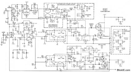
In this circuit, a 2-MHz clock is divided by eight ht U1, providing a stable 250-kHz carrier. Q1 and Q2 buffer the clock and provide a low-impedance drive for op amp U4, which is a high-gain amplifier and integrator. U4 accepts audio inputs and converts the 250-kHz square wave into a triangular wave. The summed audio and triangular-wave signal is applied to the input of comparator U7, where it is compared with a dc reference to produce a pulse-width modulated signal at the output of U7.The output devices switch between the + 50 V and -50 V rails in a complementary fashion, driving the output filter that is a sixth-order Butterworth low-pass type, which demodulates the audio and attenuates the carrier and high frequency components.Feedback is provided Rf; amplifier gain is RfRi.
Specifications: 200 W continuous power into a 4-Ω load; 20 to 20 kHz frequency response +0.5, -1.0 dB at 200 W; TED, IMD 0.5% at 200 W; 1.5-V rms input for rated output; 69 dB S/N ratio, A weighting; 6.6-V ms slew rate. (View)
View full Circuit Diagram | Comments | Reading(4243)
OSCILLOSCOPE_PREAMPLIFIER
Published:2009/7/9 2:02:00 Author:May
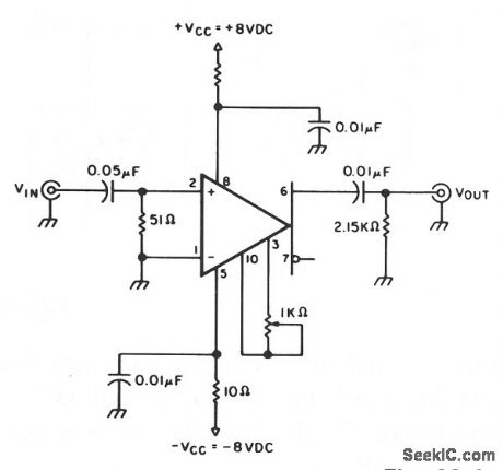
This circuit provides about 20 dB voltage gain with a frequency range from 0.5 to 50 MHz. You can extend the low-frequency response of this circuit by increasing the value of the 0.05μF capacitor-or try removing the capacitor. This circuit delivers a particularly small level of input noise, measured at approximately 20 μA over a bandwidth range of 15 MHz.
Calibrate the gain by adjusting the gain potentiometer connected between pins 3 and 10, then adjust the 1-KΩ trimmer potentiometer for an exact voltage gain of 10; this helps preserve the scale factor of the oscilloscope. (View)
View full Circuit Diagram | Comments | Reading(0)
ADD_ON_SCOPE_MULTIPLEXER
Published:2009/7/9 2:01:00 Author:May
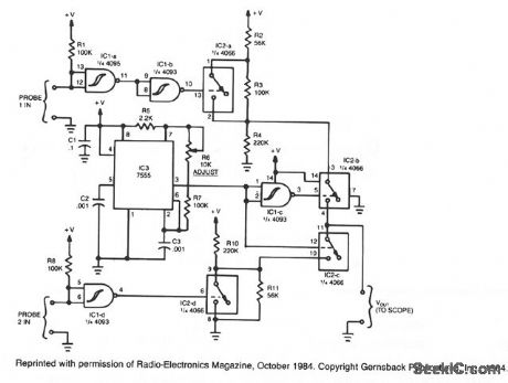
The operation of the unit revolves around three ICs: a 4093 quad NAND Schmitt trigger, a 4066 quad analog switch, and a 7555 timer. When a high is fed to probe 1 in, it is inverted to IC1a and once again by IClb, so that the input to IC2a is high. That high causes the stoitch contacts in IC2a to close. With the contacts closed, a high-level output is presented to the input of IC2b. The high output is fed to probe 2 in.That signal is then inverted by ICld and routed to IC2d, causing its contacts to open, and the unit to output a logic-level high. The output of IC2d is then fed to IC2c. (View)
View full Circuit Diagram | Comments | Reading(1361)
PORTABLE_AMPLIFIER
Published:2009/7/9 2:00:00 Author:May
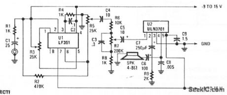
U1, an FET op amp needs a bipolar voltage at pins 4 and 7 with a common ground for optimum gain.You can calculate the gain by dividing R2 by R1. Zero-set balance can be had through pins 1 and 5 through R3. Put a voltmeter between pin 6 and ground and adjust R3 for zero voltage. Once you've established that, you can measure the ohmic resistance at each side of R3's center tap and replace the potentiometer with fixed resistors. R6, R7, RS,and C3 form a tone control that will give you added bass boost, if needed. (View)
View full Circuit Diagram | Comments | Reading(783)
SCOPE_SENSITIVITYAMPLIFIER
Published:2009/7/9 1:59:00 Author:May
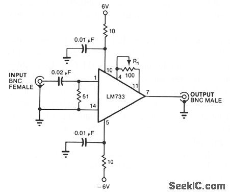
This circuit provides 20 ±0.1 dB voltage gain from 0.5 to 25 MHz and ±3 dB from 70 kHz to 55 MHz. An LM733 video amplifter furnishes a low input-noise spec, 10-μV typical, measured over a 15.7-MHz bandwidth. The scale factor of the instrument can be preserved by using a trimmer R1 or a selected precision resistor, to set the circuit's voltage gain to exactly 100. (View)
View full Circuit Diagram | Comments | Reading(3247)
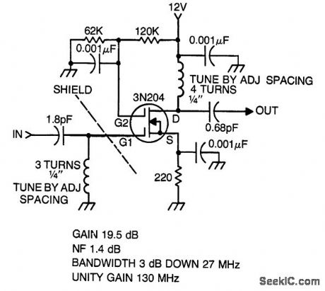
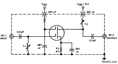
200_MHz_RF_post_amplifier_usmg_two_3N204_dual_gate_MOSFETs
Published:2009/7/20 8:46:00 Author:Jessie
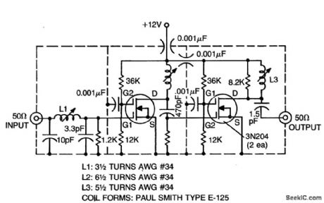
200 MHz RF post amplifier usmg two 3N204 dual-gate MOSFETs (courtesy Texas Instruments Incorporated). (View)
View full Circuit Diagram | Comments | Reading(839)
50_W_AUDIO_POWER_AMPLIFIER
Published:2009/7/9 1:57:00 Author:May
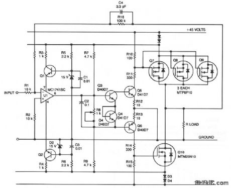
This audio amplifier design approach employs TMOS Power FETs operating in a complementary common-source configuration. They are biased to cutoff, then turn on very quickly when a signal is applied.The advantage of this approach is that the output stage is very stable from a thermal point of view.U1 is a high slew-rate amp that drives Q3, Q4,and Q6 (operating class AB) providing level transition for the output stage consisting of Q7, Q8, Q9,and Q10. The positive temperature coefficient of the TMOS device enables parallel operation of Q7, Q8, and Q9 and provides a higher power complementary device for Q10. These TMOS Power FETs must be driven from a low-source impedance of 1000, in order to actually obtain high turn-on speeds. (View)
View full Circuit Diagram | Comments | Reading(974)
LOW_DISTORTION_AMPLIFIER_COMPRESSOR
Published:2009/7/9 1:53:00 Author:May
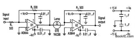
Designers can build a 15-dB compressor with a miniature lamp and a current-feedback amplifier. The circuit possesses extremely low distortion at frequencies above the lamp's thermal time constant. This means that distortion is negligible from audio frequencies to beyond 10 MHz. There's also relatively little change in phase versus gain compared to other automatic gain-control circuits. Lastly, the circuit has many instrumentation, audio, and high-frequency applications as a result of its low distortion and small phase change.
The AD844 op amp is a perfect fit for this application because it's a current-feedback amplifier. Each stage of the circuit, U2, lamp, and feedback resistor compresses an ac signal by over 15 dB (see the fig-ure). Cascading a number of stages delivers higher compression ranges.
Op amp U1 operates as a unity-gain buffer to drive the input to the compressor. However, U1 is optional if a low-impedance signal source is used. The lamp's resistance will increase with temperature, which reduces the ratio of resistor R3 to the resistance of the lamp. This ratio reduces the gain of U2. The lamp's cold resistance should be greater than the input resistance of U2 (more than 50Ω) for proper oper-ation. The lamp's resistance will change slightly for low input levels. Therefore, the ratio of R3 to the resistance of the lamp and the gain of U2 stays high. (View)
View full Circuit Diagram | Comments | Reading(1591)
LOE_DISTORTION_VIDEO_BUFFER
Published:2009/7/9 1:49:00 Author:May
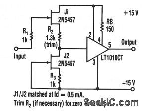
This buffer amplifier's overall harmonic distortion is a low 0.01% or less at 3-V rms output into a 500-Ω load with no overall feedback. The LT1010CT offers a 100 V/μs slew rate, a 20 MHz video bandwidth, and 100 mA of output. A pair of JFETs, J1 and J2 are preselected for a nominal match at the bias level of the linearized source-follower input stage, at about 0.5 mA. The sourcebias resistor, R2, of J1 is somewhat larger than R3 so that it can drop a larger voltage and cancel the LT1010CT's offset. J1 and J2 provide an untrimmed dc offset of ± 50 mV or less. Swapping J1 and J2 or trimming the R2 value can give a fmer match.The circuit's overall harmonic distortion is low: 0.01% or less at 3-V rms output into a 500-Ω load with no overall feedback. The circuit's response to a ±5 V, 10 kHz square-wave input, band-limited to 1 μs, has no overshoot. If needed, setting bias resistor RB lower can accommodate even steeper input-signal slopes and drive lower impedance loads with high linearityi The main trade-off for both objectives is more power dissipation. A secondary trade-off is the need for retrimming the source-bias resistor, R2. (View)
View full Circuit Diagram | Comments | Reading(787)
ONE_STAGE_TRANSISTOR_VIDEO_AMPLIFIER
Published:2009/7/20 20:45:00 Author:Jessie
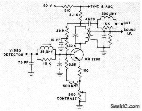
Overcomes Miller capacitance effect that normally causes excessive high-frequency rolloff. Intended for 12-inch and smaller b-w receivers, and provides direct cathode-ray drive. Bandwidth is 2 Mc. Uses MM2260 npn high-voltage silicon epitaxial transistor.-D. L. Wollesen, A Single Stage Video Ampli6er, Motorola Application Note AN-186, Feb. 1966. (View)
View full Circuit Diagram | Comments | Reading(754)
75_Ω_VIDEO_PULSE_AMPLIFIER
Published:2009/7/9 1:35:00 Author:May
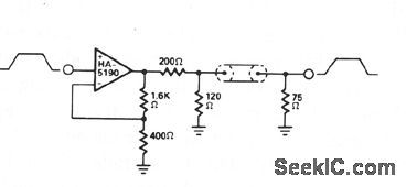

HA-5190 can drive the 75-Ω coaxial cable with signals up to 2.5 V pk-pk without the need for cur-rent boosting. In this circuit, the overall gain is approximately unity because of the impedance matching network. (View)
View full Circuit Diagram | Comments | Reading(702)
450_432_MHz_PF_amplifier_using_a_3N204_dual_gate_MOSFET
Published:2009/7/20 23:30:00 Author:Jessie
450/432 MHz PF amplifier using a 3N204 dual-gate MOSFET(courtesy TexasInstruments Incorporated). (View)
View full Circuit Diagram | Comments | Reading(1163)
PHASE_SPLTTING_PREAMP
Published:2009/7/20 22:51:00 Author:Jessie
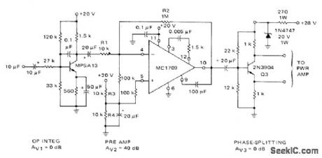
Uses Motorola MPSA13 operational integrator to provide 90° phase shift for MC1709 inverting opamp, with single-ended output complemented by phase splitting amplifier to provide push-pull drive for power amplifier of 115-V 60-Hz senvomotor, Voltage gain is about 40 dB.-A Pshaenich, Servo Motor Drive Amplifiers, Motorola, Phoenix,AZ,1972,AN-590. (View)
View full Circuit Diagram | Comments | Reading(1382)
903_MHz_LINEAR_AMPLIFIERS
Published:2009/7/9 1:12:00 Author:May
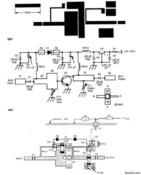

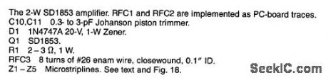
Two W output can be produced by this circuit designed for the 902- to 928-MHz amateur band. As shown in the figures, much of the circuitry is in the form of PC board traces. (View)
View full Circuit Diagram | Comments | Reading(774)
Linear_amplitude_modulator_circuit_using_an_AD534_multiplier_divider_chip
Published:2009/7/20 22:50:00 Author:Jessie
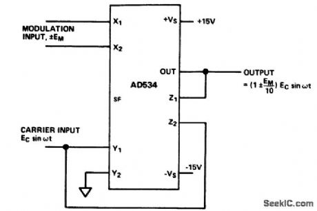
Linear amplitude modulator circuit using an AD534 multiplier/divider chip(courtesy Analog Devices,Inc.). (View)
View full Circuit Diagram | Comments | Reading(2533)
10_to_15_W_ATV_LINEAR_AMPLIFIER
Published:2009/7/9 1:07:00 Author:May
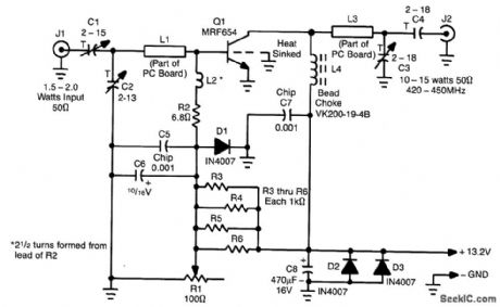
This amplifier is useful for applications where a 10- to 15-W peak-envelope-power (PEP) signal is needed in the 420- to 520-MHz range. C1, C2, and L1 form a matching network for amplifter Q1. L3, C3, and C4 form an output matching network for a 50-Ω load. L2, R2, D1, and R3 through R6with bias adjust R1) form a biasing network for Q1. D2 and D3 provide polarity protection for Q1, which must be heat-sinked. A kit of all parts including case and PC board is available from North Country Radio, P.O. Box 53, Wykagyl Station, New Rochelle, NY 10804. (View)
View full Circuit Diagram | Comments | Reading(1097)
6_m_100_WILNEAR_AMPLIFIER
Published:2009/7/9 1:05:00 Author:May
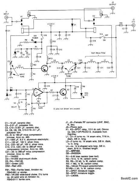

100 W output at 50 MHz is available from this circuit. UI and Q2 form a T-R relay driver, switching the amplifier on when RF input at J1 is sensed. During receive periods, J1 and J2 are directly connected. A 13.8-V supply is required for this amplifier. (View)
View full Circuit Diagram | Comments | Reading(982)
105_MHz_gate_2_controlled_RF_amplifier_using_a_TIS152_dual_gate_MOSFET
Published:2009/7/20 22:46:00 Author:Jessie
105 MHz gate-2-controlled RF amplifier using a TIS152 dual-gate MOSFET (courtesy Texas Instruments Incorporated). (View)
View full Circuit Diagram | Comments | Reading(908)
| Pages:103/250 At 20101102103104105106107108109110111112113114115116117118119120Under 20 |
Circuit Categories
power supply circuit
Amplifier Circuit
Basic Circuit
LED and Light Circuit
Sensor Circuit
Signal Processing
Electrical Equipment Circuit
Control Circuit
Remote Control Circuit
A/D-D/A Converter Circuit
Audio Circuit
Measuring and Test Circuit
Communication Circuit
Computer-Related Circuit
555 Circuit
Automotive Circuit
Repairing Circuit