
Amplifier Circuit
Index 110
HALL_EFFECT_COMPASS
Published:2009/7/7 7:32:00 Author:May
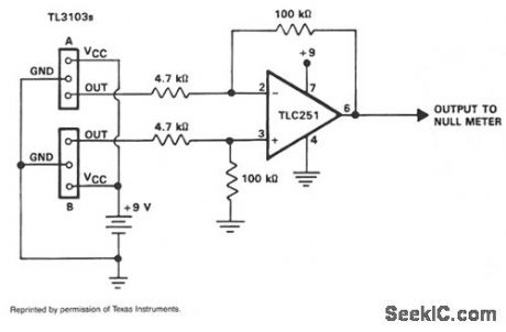
The TL3103 linear Hall-effect device can be used as a compass. By definition, the north pole of a magnet is the pole that is attracted by the mag-netic north pole of the earth. The north pole of a magnet repels the north-seeking pole of a compass. By convention, lines of flux emanate from the north pole of a magnet and enter the south pole, The cir-cuit of the compass is shown. By using two TL3103 devices instead of one, we achieve twice the sensitivity. With each device facing the opposite direc-tion, device A would have a position output while the output of device B would be negative with respect to the zero magnetic field level. This gives a differential signal to apply to the TLC251 op amp. The op amp is connected as a difference amplifier with a gain of 20. Its output is applied to a null meter or a bridge balance indicator circuit. (View)
View full Circuit Diagram | Comments | Reading(2387)
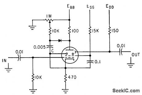
DYNODE_TO_GRID_POSITIVE_FEEDBACK
Published:2009/7/21 8:11:00 Author:Jessie
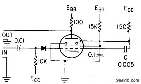
Produces negative output pulse across plate load of secondary-emission pentode. Feedback is from dynode to control grid, rather than from plate to cathode. Diode insures that feedback pulse does not affect other circuits, und makes feedback nearly independent of input generator impedance. Used in high-speed, short. duration pulse work.-E. J. Martin, Jr., How to Use the Secondary-mission Pentode, Electronics, 33:41, p 60-63. (View)
View full Circuit Diagram | Comments | Reading(646)
VOLTAGE_SENSING
Published:2009/7/21 8:11:00 Author:Jessie
Unijunction transistor is triggered when input signal is slightly positive, and then generates pulses as long us input remains positive. Output con be used to trigger flip-flop or turn on scr's.-D. V. Jones, Quick-On-The-Trigger Design, Electronics, 38:12, p 105-110. (View)
View full Circuit Diagram | Comments | Reading(754)
SERIES_SCHMITT
Published:2009/7/21 8:10:00 Author:Jessie
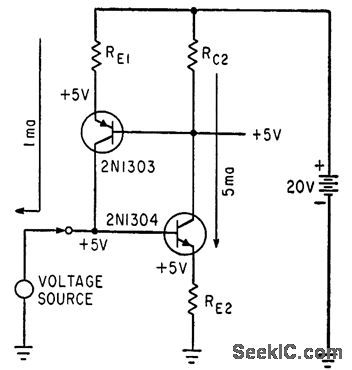
Complementary transistors are either both on or both off, conserving power for trigger, comparator, flip-flop, one shot, and oscillator applications. With 20,v supply, RB1 is 15 K, RC2 is 3K, and RE2 is 1K.-J. K. Skilling, New Complementary Transistors make Series Schmitt Circuits Practical, Electronics, 35:35, p 52-53. (View)
View full Circuit Diagram | Comments | Reading(1417)
175_SCHMITT
Published:2009/7/21 8:09:00 Author:Jessie
Use of inexpensive transistors and fixed resistors in place of potentiometers keeps cost low. Hysteresis control R2 and trigger level control R3 are optional. Output is 8 v peak to peak at 50 kc.-A. Pacela, Low-Cost Schmitt Trigger Reduces Hysteresis, Electronics, 38:24, p 63-64. (View)
View full Circuit Diagram | Comments | Reading(618)
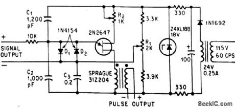
FREQUENCY_COUNTER_PREAMP
Published:2009/7/7 6:30:00 Author:May
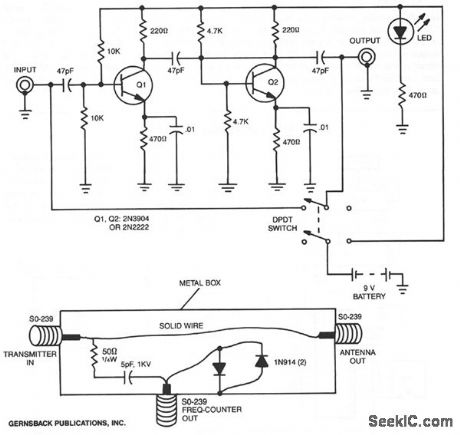
By using the preamplifier with a short length of shielded cable and clip leads, signals that generally could not generate a readout, generate precise and stable readouts on the counter. The DPDT switch is used to bypass the circuit when amplification is not needed. The preamplifier can also be used for other purposes. For example, the unit was also tested as a receiver preamplifier and increased received signal strength about 6 S-units at 30 MHz. A line tap can be used to measure the frequency directly at the output of a transmitter. The entire circuit for that consists of two diodes, one resistor, and one capacitor. The line tap simply picks a low-amplitude signal for measurement by the frequency counter. The tap can be connected to transmitters with an output power of between 1 and 250 W. (View)
View full Circuit Diagram | Comments | Reading(3731)
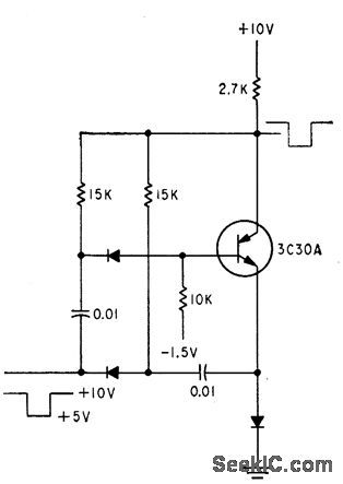
COLLECTOR_TRIGGERING_WITH_TRIG0ER_AM_PLIFIER
Published:2009/7/21 9:19:00 Author:Jessie
Used in early stages of counter to increase speed, while permitting automatic assembly in all stages. For 1-Mc trigger rate, less than 1 v of positive trigger amplitude is needed.- Transistor Manual, Seventh Edition, General Electric Co., 1964, p 198. (View)
View full Circuit Diagram | Comments | Reading(640)
BASE_TRIGGERED_FLIP_FLOP
Published:2009/7/21 9:14:00 Author:Jessie
Maximum trigger rate for steering circuit exceeds 5 Mc with negative trigger pulse amplitude from 0.75 to 2 v. Requires less trigger energy than collector triggering but more accurately controlled trigger amplitude.- Transistor Manual, Seventh Edition, General Electric Co., 1964, p 197. (View)
View full Circuit Diagram | Comments | Reading(675)
SENSE_AMPLIFIER
Published:2009/7/21 9:13:00 Author:Jessie
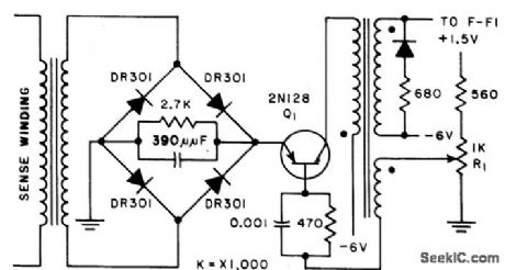
Blocking-oscillator transistor amplifier is triggered by output of diode bridge network. Rectification assures that readout voltages of both polarities are sensed.Diodes attenuate small signals greatly relative to large signals, increasing signal-noise ratio at rectifier output to about 20:1.-C. S. Warren, W. G. Rumble, and W. A. Helbig, Transistorized Memory Monitors Earth Satellite, Electronics, 31:3, p 66-70.
(View)
View full Circuit Diagram | Comments | Reading(1)
LC_PULSE_GENERATOR
Published:2009/7/21 9:12:00 Author:Jessie
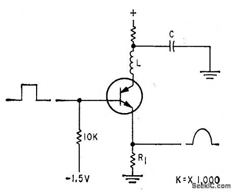
Provides half-sinusoid output determined by L and C, when pnpn unit is triggered on by low-level positive pulse applied to its base.-J. B. Hangstefet and L. H. Dixon, Jr., Triggered Bistable Semiconductor Circuits, Electronics, 32:35, p 58-60. (View)
View full Circuit Diagram | Comments | Reading(894)
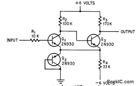
NONCUTOFF_SCHMITT
Published:2009/7/21 9:07:00 Author:Jessie
Both amplifiers are always connected to their current sources, hence are never cut off and can operate in optimum region, with no risk of damage by inverse base-emitter voltage. Output voltage alternates between two levels.-H. Inose, Y, Yoshida, and H. Tada, Noncutoff Circuits Improve Trigger Switching, Electronics, 35:30, p 36-39. (View)
View full Circuit Diagram | Comments | Reading(691)
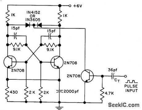
PNPN_FLIP_FLOP_BINARY_COUNTER
Published:2009/7/21 9:06:00 Author:Jessie
Negative trigger pulses produce 2:1 operation. Con be driven from identical flip-flop or from collector of npn silicon transistor.-J. B. Hang-stefer and L. H. Dixon, Jr., Triggered Bistable Semiconductor Circuits, Electronics, 32:35, p 58-60. (View)
View full Circuit Diagram | Comments | Reading(668)
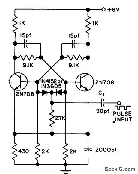
VARIABLE_SENSITIVITY_TRIGGER
Published:2009/7/21 9:06:00 Author:Jessie
Biased diode in feedback circuit prevents regeneration.Feedback cannot occur until negative-going pulse greater then bias appears at plate of secondary-emission pentode. Diode bias varies sensitivity, allowing use as pulse-height discriminator also.-E. J. Martin, Jr., How to Use the Secondary-Emission Pentacle, Electronics, 33:41, p 60-63. (View)
View full Circuit Diagram | Comments | Reading(652)
NEGATIVE_PULSE_TRIGGER
Published:2009/7/21 9:05:00 Author:Jessie
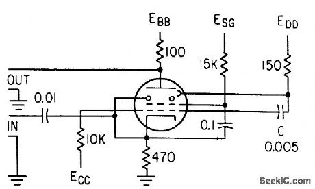
Diode is not necessary in input circuit of secondary-emission pentode, since feedback is from dynode to control grid and negative trigger pulse is impressed on cathode. Used in high-speed, short-duration pulse work.-E. J. Martin, Jr., How to Use the Secondary-Emission Pentode, Electronics, 33:41, p 60-63. (View)
View full Circuit Diagram | Comments | Reading(810)
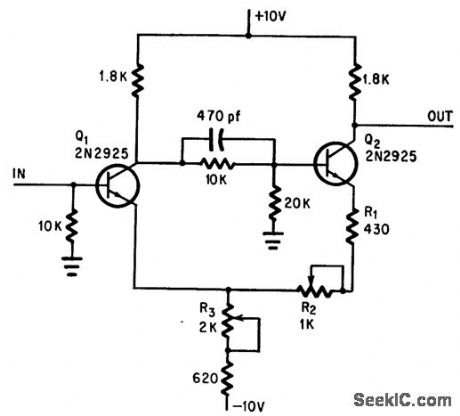
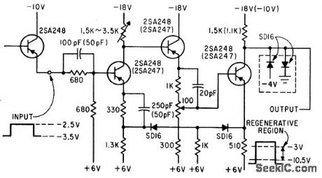
DIODE_COUPLED_SCHMITT
Published:2009/7/21 9:05:00 Author:Jessie
Uses include pulse width modulation of d-c voltage for switching amplifiers, wave shaping, and voltage or current monitoring. Low dynamic resistance of diode formed by Q2 keeps hysteresis (difference between turn-on and turn-off) down to 10 mv.-D. D. Robinson, Diode. Coupled Schmitt Trigger, Electronics, 37:31, p 50-51.
(View)
View full Circuit Diagram | Comments | Reading(796)
LOW_COST_HIGH_LEVEL_PREAMP_AND_TONE_CONTROL_CIRCUIT
Published:2009/7/7 5:34:00 Author:May
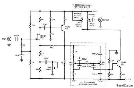
This preamp and tone control uses the JFET to its best advantage; as a low noise high input impedance device. All device parameters are noncritical, yet the circuit achieves harmonic distortion levels of less than 0.05% with a S/N ratio of over 85 dB. The tone controls allow 18 dB of cut and boost; the amplifier has a 1-V output for 100-mV input at maximum level. (View)
View full Circuit Diagram | Comments | Reading(1924)
_TONE_CONTROL_AUDIO_AMPLIFIER
Published:2009/7/7 5:32:00 Author:May
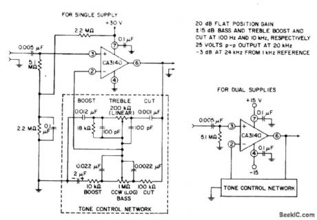


The circuit makes excellent use of the high slew rate, wide bandwidth, high input impedance, and high-output voltage capability of the CA3140 BiMOS op amp. The wideband gain of this circuit is equal to the ultimate boost or cut plus one, in this case a gain of eleven. For 20-dB boost or cut, input loading is essentially equal to the resistance from terminal 3 to ground.
(View)
View full Circuit Diagram | Comments | Reading(822)
143_156_MHz_80_W_AMPLIFIER
Published:2009/7/7 4:47:00 Author:May
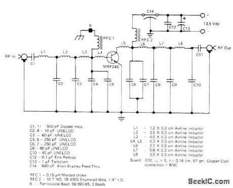
Single transistor mounted on heavy heatsink provides about 9.4-dB gain. 8-W drive at 13.5 VDC produces full output power. Series tuning inductors are printed striplines with ground plane removed beneath them; report gives designs for photomasks. Transistor will withstand 20:1 VSWR at all phase angles,-T. Bishop, A Single-Device, 80-Watt, 50-Ohm VHF Amplifier, Motorola, Phoenix, AZ, 1978, EB-46. (View)
View full Circuit Diagram | Comments | Reading(1751)
300_mW_25_MHz_AMPLIFIER
Published:2009/7/7 4:25:00 Author:May
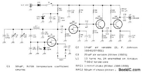
Uses quarter-wavelength transmission line T3 in place of parallel-tuned traps to pass even-harmonic currentfreelywh"e blocking odd harmonics Circuit canbe adapted to 300-mW、fvalkie-talkie for 6 or 10meters At 25 MHz、efficiency is 73%,-F, H,Raab,High-Efficiency RF Power Amplifiers,Ham Radio,Oct 1974,p 8-29. (View)
View full Circuit Diagram | Comments | Reading(743)
LED_FREQUENCY_COMPARATOR
Published:2009/7/7 4:10:00 Author:May
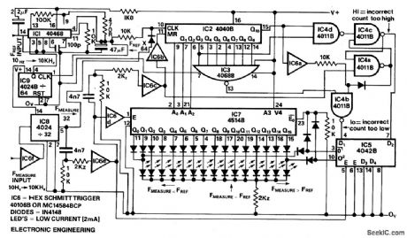
The circuit provides unambiguous LED + or - bar readout with steps of 0.1%. The reference frequency is multiplied by the PLLIC1 and divider IC9 to output 64 x F (ref) and this is then gated by dividing F (measure) by 32 in IC8 thus is F (ref) -(measure) then IC2 counts 1024 pulses. Should the count be more than 1031 than the t latch IC4c/IC4a is set to indicate count too high (F (measure) F (ref)) and if the count is less than 1017 then IC3/IC4b indicate count too low (F(measure) F (ref). These signals are latched by IC5 at the end of each period by the latch signal from IC6e.When the two frequencies are within + or - 0.670 the LSB's of the counter IC2 are decoded and latched by IC7 and displayed on LED's IC6c resets the counter after latching the data. (View)
View full Circuit Diagram | Comments | Reading(1397)
| Pages:110/250 At 20101102103104105106107108109110111112113114115116117118119120Under 20 |
Circuit Categories
power supply circuit
Amplifier Circuit
Basic Circuit
LED and Light Circuit
Sensor Circuit
Signal Processing
Electrical Equipment Circuit
Control Circuit
Remote Control Circuit
A/D-D/A Converter Circuit
Audio Circuit
Measuring and Test Circuit
Communication Circuit
Computer-Related Circuit
555 Circuit
Automotive Circuit
Repairing Circuit