
Filter Circuit
Index 15
FULL_WAVE_RECTIFIER_AND_AVERAGING_FILTER
Published:2009/6/25 22:45:00 Author:May
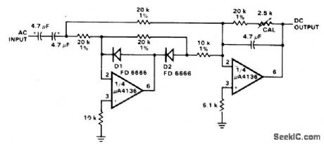
View full Circuit Diagram | Comments | Reading(660)
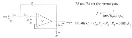
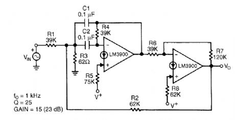
ACTIVE_CW_AUDIO_FILTER
Published:2009/6/24 2:16:00 Author:May
The audio filter shown has a bandpass of 200 Hz centered on 700 Hz. Resistors are 1% tolerance and capacitors should be 5% tolerance. (View)
View full Circuit Diagram | Comments | Reading(959)
Level 4 Telecom Filter Circuit of uA741 Op-amp
Published:2011/7/22 21:56:00 Author:Michel | Keyword: Op-amp, Level 4, Telecom, Filter Circuit
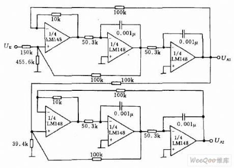
The above circuit can use common calculation formula and then the total requirements are divided into several sections:Q1=0.541,Q2=1.306.This circuit adopts LM148 or 741 four operational amplifier. (View)
View full Circuit Diagram | Comments | Reading(932)
PROGRAMMABLE_GAIN_NONINVERTINGAMPLIFIER_WITH_SELECTABLE_INPUTS
Published:2009/6/23 2:08:00 Author:May
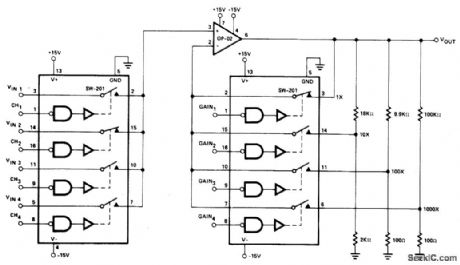
View full Circuit Diagram | Comments | Reading(0)
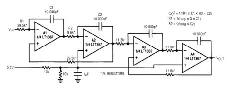
1_kHz_4TH_ORDER_BUTTERWORTH_FILTER
Published:2009/6/19 2:33:00 Author:May
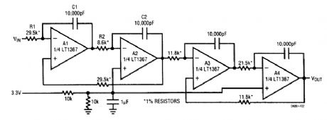


The filter is a simplified state variable architecture consisting of two cascaded 2nd-order sections. Each section uses the 360° phase shift around the two op-amp loop to create a negative sum-ming junction at Al's positive input. The circuit has low sensitivities for center frequency and Q, which are set with the following equations:where,The dc bias applied to A2 and A4, half supply, is not needed when split supplies are available.The circuit swings rail-to-rail in the passband making it an excellent anti-aliasing filter for A/Ds. The amplitude response is flat to 1 kHz then rolls off at 80 dB/decade. (View)
View full Circuit Diagram | Comments | Reading(1240)
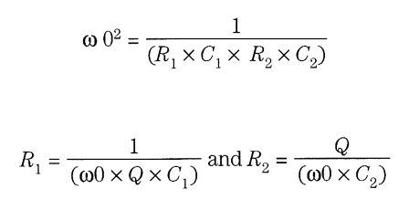
RC_NOTCH_FILTER
Published:2009/6/19 2:31:00 Author:May
View full Circuit Diagram | Comments | Reading(814)
ACTIVE_HIGH_PASS_FILTER
Published:2009/6/19 2:30:00 Author:May
View full Circuit Diagram | Comments | Reading(0)
SALLEN_KEY_LOW_PASS_FILTER
Published:2009/6/19 2:30:00 Author:May
View full Circuit Diagram | Comments | Reading(735)
BANDPASS_FILTER
Published:2009/6/19 2:29:00 Author:May
View full Circuit Diagram | Comments | Reading(0)
20_kHz_BUTTERWORTH_ACTIVE_FILTER
Published:2009/6/19 2:29:00 Author:May

This filter will be useful for anti-aliasing or band limiting in an audio system.The op amp is a Linear Technology, LT1124,LT1355,or LT1169. (View)
View full Circuit Diagram | Comments | Reading(910)
VSB_FILTER_FOR_LM2889
Published:2009/6/19 2:27:00 Author:May
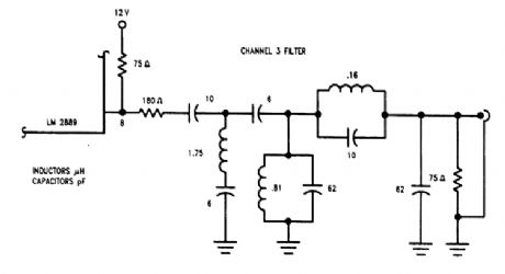
This filter is for CH3, in order to get a vestigial sideband TV signal. It is designed for 75-Ω im-pedance levels. (View)
View full Circuit Diagram | Comments | Reading(769)
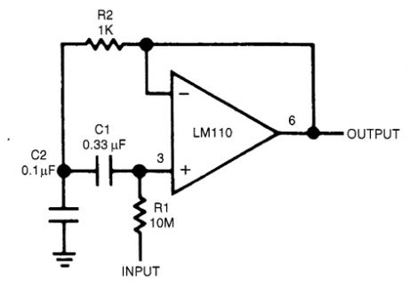
VOLTAGE_CONTROLLED_LOW_PASS_FILTER
Published:2009/6/19 2:26:00 Author:May
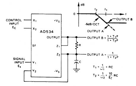
The voltage at Output A, which should be unloaded by a follower, responds as though ES were di-rected to the RC filter, but the filter's break frequency were proportional to Ec[i.e,.=Ec/(20πRC)] The frequency response has a break at f2; and the 6-dB/octave rolloff. The voltage at Output B has the same response, up to [f1 (f = 1/(20πRC)], then levels off at a constant attenuation of f2/f1 = Ec\10.For example, if R = 8kΩ, C = 0.002μF, Output A has a pole at 100 Hz to 10 kHz and can be loaded.The circuit can be converted to high-pass by interchanging C and R. (View)
View full Circuit Diagram | Comments | Reading(1)
DIGITAL_COMB_FILTER
Published:2009/6/19 2:18:00 Author:May
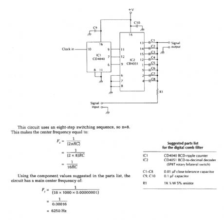
View full Circuit Diagram | Comments | Reading(919)
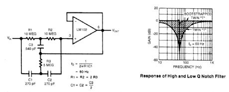
ADJUSTABLE_Q_NOTCH_FILTER
Published:2009/6/19 2:17:00 Author:May
This figure shows a circuit where the Q can be varied from 0.3 to 50. A fraction of the output is fed back to R3 and C3 by a second voltage follower, and the notch Q is dependent on the amount of signal fed back. A second follower is necessary to drive the twin T from a low-resistance source so that the notch frequency and depth will not change with the potentiometer setting. (View)
View full Circuit Diagram | Comments | Reading(0)
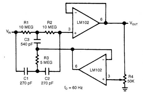
HIGH_Q_NOTCH_FILTER
Published:2009/6/19 2:16:00 Author:May
This shows a twin T network connected to an LM102 to form a high Q, 60-Hz notch filter. The Junction of R3 and C3: which is normally connected to ground, is bootstrapped to the output of the follower. Because the output of the follower is a very low impedance, neither the depth nor the frequency of the notch change; however, the Q is raised in proportion to the amount of signal fed back to R3 and C3. (View)
View full Circuit Diagram | Comments | Reading(0)
SINGLE_33_V_SUPPLY_4_POLE_STATE_VARIABLE_FILTER
Published:2009/6/19 2:09:00 Author:May
View full Circuit Diagram | Comments | Reading(636)
TWO_OP_AMP_BANDPASS_FILTER
Published:2009/6/19 2:08:00 Author:May


This circuit uses only two capacitors.The amplifier on the right supplies a controlled amount of characteristics. Resistors R5 and R8 are used to bias the outvoltage of the amplifiers at V+/2. (View)
View full Circuit Diagram | Comments | Reading(1)
ACTIVE_LOW_PASS_FILTER
Published:2009/6/19 2:04:00 Author:May
This circuit has a rolloff of 6 dB/Octave. (View)
View full Circuit Diagram | Comments | Reading(0)
PROGRAMMABLE_ANALOG_FILTER
Published:2009/6/19 2:03:00 Author:May
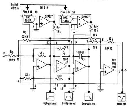
The circuit in the figure shows how an analog, digitally programmable filter can be built using a UAF42. This monolithic, state-variable active filter chip provides a two-pole filter building block with low sensitivity to extemal component variations. It eliminates aliasing errors and clock feed though noise common to switched-capacitor filters. Low-pass, high-pass, bandpass, and notch (band-reject) outputs are available. (View)
View full Circuit Diagram | Comments | Reading(1771)
SHORTWAVE_INTERFERENCE_TRAP
Published:2009/6/19 2:01:00 Author:May
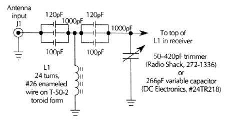
Build this interference trap to help block strong shortwave, broadcast, and FM stations from corning in on the shortwave bands. (View)
View full Circuit Diagram | Comments | Reading(977)
| Pages:15/21 1234567891011121314151617181920Under 20 |
Circuit Categories
power supply circuit
Amplifier Circuit
Basic Circuit
LED and Light Circuit
Sensor Circuit
Signal Processing
Electrical Equipment Circuit
Control Circuit
Remote Control Circuit
A/D-D/A Converter Circuit
Audio Circuit
Measuring and Test Circuit
Communication Circuit
Computer-Related Circuit
555 Circuit
Automotive Circuit
Repairing Circuit