
Filter Circuit
Index 19
Typical Appied Circuit Diagram of LM1036N Integrated Circuit
Published:2011/6/15 8:15:00 Author:Vicky | Keyword: Typical Applied Circuit Diagram
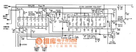
Picture: Typical Applied Circuit of LM1036N Integrated Circuit
Typical Applied Circuit
Typical Appied Circuit Diagram of LM1036N Integrated Circuit is as shown in the picture. (View)
View full Circuit Diagram | Comments | Reading(2117)
Internal Circuit Block Circuit Diagram of LM1203 Integrated Circuit
Published:2011/6/15 8:15:00 Author:Vicky | Keyword: Internal Circuit Block Circuit Diagram
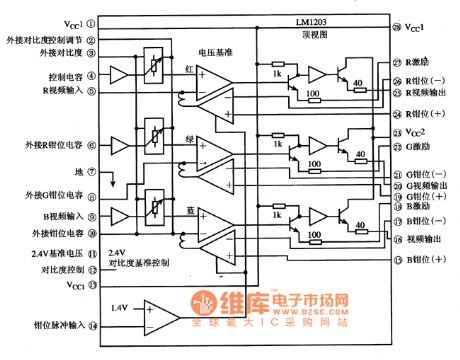
Picture:Internal CircuitBlock Circuit Diagram of LM1203 Integrated Circuit
Functions and Characteristics
The interior of LM1203 integrated circuit is made of three circuits of the same functions, including video small-signal processing circuit, contrast basic control circuit and clamp pulse, and some other adjunct circuits. The internal circuit block diagram is as shown in the picture. (View)
View full Circuit Diagram | Comments | Reading(1323)
Typical Applied Circuit Diagram of LM4610 Integrated Circuit
Published:2011/6/15 8:09:00 Author:Vicky | Keyword: Typical Applied Circuit Diagram
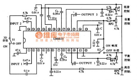
Typical Applied Circuit
Typical applied circuit diagram of LM4610 integrated circuit is shown in the following picture. The LM4610 circuit uses 4 potentiometers MU-M as bass control, volume control, treble control and balance control respectively.
Hint: Left/Right acoustical signal enter LM4610 from (2) pin and (23) pin, get out from (10) pin and (15) pin after processed by the sound volume, tone, balance and 3D audio, and then go to the post-stage circuit. It can be justified that whether LM4610 works regularly by this four pins.
(View)
View full Circuit Diagram | Comments | Reading(3213)
Typical Applied Circuit Diagram of LM8363D/DH Integrated Circuit
Published:2011/6/15 8:07:00 Author:Vicky | Keyword: Typical Applied Circuit Diagram of LM8363D/DH Integrated Circuit,
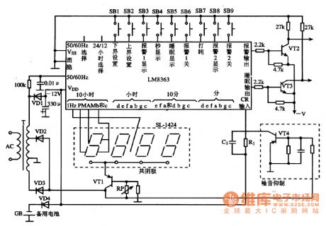
Picture: Typical Applied Circuit of LM8363D/DH integrated circuit
Typical applied circuitTypical applied circuit diagram of digital circuit ,which is composed of LM8363D/DH integrated circuit, is as shownin the picture.
Hint: LM8363 integrated circuit can be thereserve when the power is cut off, and selection method of the value reuired by the osillator is listed below:
grade of 60Hz:R1=130k、C1=0.0068μF,f。=1.92kHz;
grade of 50Hz:R1=150k、C1=0·0068μF,f。=1.6kHz. (View)
View full Circuit Diagram | Comments | Reading(2628)
Voice Filter Circuit of LM387
Published:2011/6/24 2:12:00 Author:Michel | Keyword: Voice, Filter Circuit
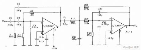
Serial Voice frequency range filter circuit is shown as above and its frequency range is 360Hz-3KHz. (View)
View full Circuit Diagram | Comments | Reading(1364)
Complementary tube double bistable circuit
Published:2011/6/30 8:09:00 Author:Fiona | Keyword: Complementary tube, double bistable
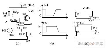
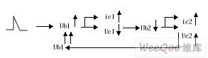
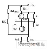
Complementary tube double bistable circuit is shown in Figure 1 (a).When it is charged tothe power supply,if there is no trigger effect,because the collector current is very small and the voltage of Rc1 and Rc2 is also small,two tubes are both off,the circuit keeps the steady state.Under the trigger pulse,assume BG1 changes from close to enlarge,and produces following the avalanche of positive feedback process.Quickly make the two tubes be saturate connected,in another steady state,capacitance C1 is accelerated capacitance,by the form 1(b) visible,uc1 is steeply down to zero,but UC2 is steeply from zero up to Ec.
(View)
View full Circuit Diagram | Comments | Reading(978)
Optical receiver circuit diagram
Published:2011/7/2 21:18:00 Author:leo | Keyword: Optical receiver circuit diagram, LA7224
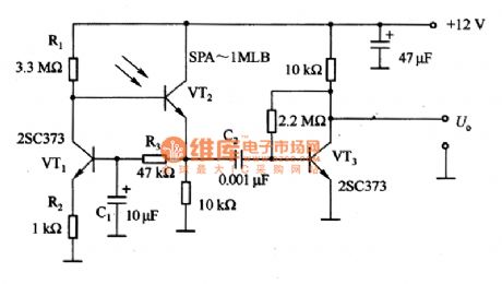
The picture shows a optical receiver circuit. In this circuit, LA7224 is a kind of front amplifier which is used to receive signals. Peak value keeping circuit, integral circuit and so on can form the integrated circuit of the same chip. The syntony circuit formed by L and G2 are used to get carrier and the carrier comes through the amplitude-limited circuit to keep the peak value (C3), by which the S/N of this circuit is improved. C4 is integral circuit and capacitor recommended is 0.0047μF. When the output voltage of the pin 1 of LA7224 is 0.3 V, VT1 is stopped and output voltage is U which is a high value. (View)
View full Circuit Diagram | Comments | Reading(1008)
LA7845N-Field scanning output integrated circuit
Published:2011/7/2 21:27:00 Author:leo | Keyword: LA7845N-Field scanning output integrated circuit
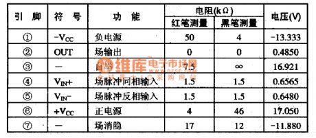
LA7845N is a kind of field scanning output integrated circuit made by Sanyo corporation which is widely used in big screen color television.
It has few peripheral components and adopts negative sources to offer the power. It does not perfect over current, overvoltage and overheating protecting circuit. Besides, the maximum output current of it is 3Ap-p and the maximum power consumption is 11W while the maximum output voltage is 40 V. The maximum source output voltage can reach 85 V. The inner circuit of this integrated circuit is shown in the picture and you can also find the pin functions and related data in it. (View)
View full Circuit Diagram | Comments | Reading(750)
High-Accuracy Pressure Amplifying Circuit Diagram
Published:2011/6/26 9:11:00 Author:Vicky | Keyword: High-Accuracy Pressure Amplifying
High-accuracy pressure amplifying circuit is mainly used in amplifying system of small sensor output signal. AD624 is amplifying circuit of high-accuracy low-noise instrument. The above picture is a high-accuracy amplifying circuit composed of AD624, and the sensor is a standard resistance straining bridge transducer. The bridge uses voltage of + 9.00V. Potentiometers R8 and R6 are used as zero setting. R6 is coarse regulation while R8 is fine regulation. The output of the amplifier can be connected to high-accuracy A/D converter directly. The number of amplifying time in the picture is 500. The signal can be amplified by a piece of AD624. (View)
View full Circuit Diagram | Comments | Reading(716)
F107 Double-Power General-Type Single-Supply Amplifier Circuit Diagram
Published:2011/6/26 9:16:00 Author:Vicky | Keyword: Double-Power General-Type Single-Supply
F107 series operational amplifier is a monolithic general-type inner complementing amplifier, with relatively low input current. It has no need of exterior complementing components, and is available in integrator, and sampling/maintaining low-frequency wave generator. The analog types or substitutions are F107MT、F207LT、F307CT、F107MD、F207LD、F307CD,Fl07MJ,F207LJ、F307CJ,F307CP,SM107,SG207,SG307,LMl07,LM207,LM307 etc. (View)
View full Circuit Diagram | Comments | Reading(776)
CF155 Double-Power High Input-Impedance Single-Supply Amplifier Circuit Diagram
Published:2011/6/26 9:22:00 Author:Vicky | Keyword: Double-Power High Input-Impedance Single-Supply
CF155 series operational amplifier’s output circuit is composed by MOSFET. Its features are: low input current, low power supply current, low power dissipation, low noise, low offset voltage, and exterior zero-setting end. It is available in high-speed integrator, sampling/maintaining circuit of quick-speed D/A converter. The analog types or substitutions are: CFl55MT、CF255LT、CF355CT、CFl55MD、CF255LD、CF355CD、CFl55MJ、CF255LJ、CF355CJ、CF355CP. The above pictures are CF155 typical applied circuit: picture(a) is inverting amplifying and zero-setting circuit, and picture(b) is differential input and zero-setting circuit. (View)
View full Circuit Diagram | Comments | Reading(707)
Typical Application Circuit of M54123 Intergrated Circuit
Published:2011/5/16 20:54:00 Author:Michel | Keyword: Application Circuit , Intergrated Circuit
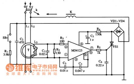
Typical Application Circuit
Typical application circuitof leakage protecter composed of M54123 IC is showed as above.
Picture:Typical Application Circuit of M54123 Intergrated Circuit
Note:China's homegrown part number of M54123 IC is SF4123 and they can be used interchangeably directly.
(View)
View full Circuit Diagram | Comments | Reading(1664)
The Inner Circuit Pane Circuit Diagram of M54123 IC
Published:2011/5/16 20:55:00 Author:Michel | Keyword: IC, Inner Circuit Pane, Ciruit Diagram
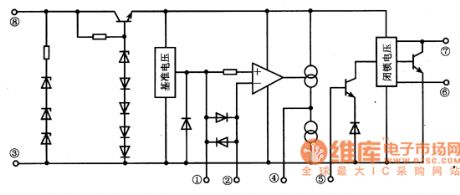
Functions and Features
M54123 IC is composed of voltage stabling circuit,voltage reference circuit,differential amplifier,lockout and output circuit etc.Its major features are as follows.
Firstly,supply voltage range is from 12-28V.Line voltage could work normally when it changes from 120V to 280V,that's to say, leakage circuit can be swtiched off reliably when line voltage is at the low point.
Secondly,operation voltage is low(4-9mv),so its zero-sequence current mutual inductor volume is small.
Thirdly,leakage operation current is steady becuase there is voltage reference.
Fourth,the actual requirements can be meet completely as the operation time less than 0.5s.The Inner Circuit Pane Circuit Diagram of M54123 IC is showed as above.
Picture:The Inner Circuit Pane Circuit Diagram of M54123 IC (View)
View full Circuit Diagram | Comments | Reading(1176)
Typical Application Circuit of M52340SP IC
Published:2011/5/16 7:13:00 Author:Michel | Keyword: IC, Application Circuit
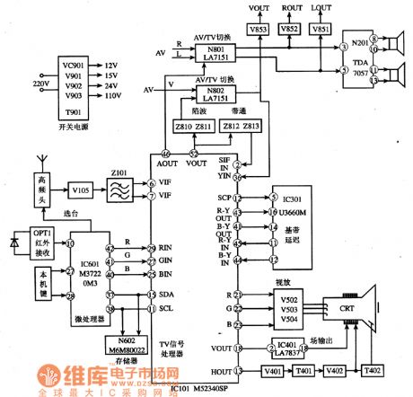
Typical Application Circuit
The typical application circuit of M52340SP IC shows as the picture.Konka F2136 color TV is a typical application example.
Picture:Typical Application Circuit of M52340SP IC
Note:If both image and sound accompaniment go wrong meanwhile ,we shuold check 38MHz intermediate sequancy signal which is high sequancy singal at first but changed into intermediate then whether it is added to ⑥ and ⑦ feet.The M52340SP circuit will be checked if the signal is normal.Typical Application Circuit of M52340SP IC (View)
View full Circuit Diagram | Comments | Reading(1181)
The Inner Circuit Pane Circuit of M52340SP IC
Published:2011/5/18 2:31:00 Author:Michel | Keyword: IC, Circuit Pane Circuit Diagram
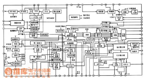

Functions and Features
M52340SP IC has IC bus control circuit,which simpilies many outer components,circuit and makes productlines more rational.That is to say,the intergrated circuit contains wave-trap,high pass filter,luminance delay line,RGB clamping circuit and adopts PLL detecting system which can deal wtih image intermediate frequency and sound intermediate frequency without sting coil.In addition,it uses delay line control,that is to say,it can recognise kinds of color tlevisions'signal frequency and field frequency.Besides,it uses line and frequency demultiplication.
(View)
View full Circuit Diagram | Comments | Reading(1254)
Typical Application Circuit of M5060-O1P IC
Published:2011/5/16 7:13:00 Author:Michel | Keyword: Application Circuit
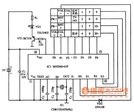
Typical Application Circuit
Remote-control emitter typical appliction circuit composed of M50560 IC is showed as above.
Picture:Typical Application Circuit of M5060-O1P IC (View)
View full Circuit Diagram | Comments | Reading(797)
Inner Circuit Pane Circuit of M50560-01P IC
Published:2011/5/18 2:32:00 Author:Michel | Keyword: Inner Circuit Pane, Circuit, IC
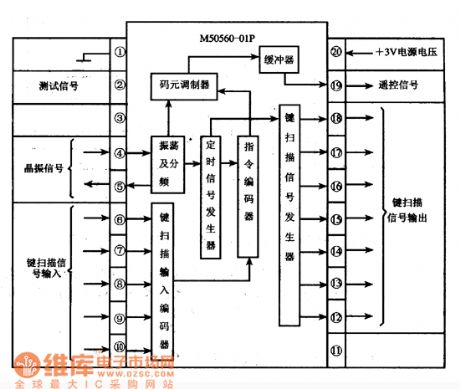
Functions and FeaturesM50560一01P contains color periodic circuit,teleswitch command encoder timing signal generator,key sweep gate generator,code element modulator,buffer and other accessory circuit.Its inner circuit pane picture is showed as above.Picture:Inner Circuit Pane Circuit of M50560-01P IC (View)
View full Circuit Diagram | Comments | Reading(981)
Typical Application Circuit of M54060 IC
Published:2011/5/17 3:38:00 Author:Michel | Keyword: Typical Application Circuit

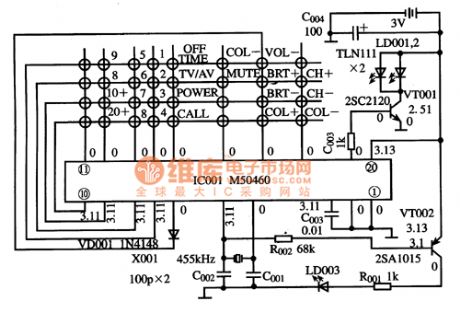

Typical Application Circuit
The remote control applied ciruit composed of M50460 IC is showed as above.
Picture:Typical Application Circuit of M50460 IC (View)
View full Circuit Diagram | Comments | Reading(811)
Typical Application Circuit of M50142P IC
Published:2011/5/18 2:28:00 Author:Michel | Keyword: Typical Application Circuit, IC
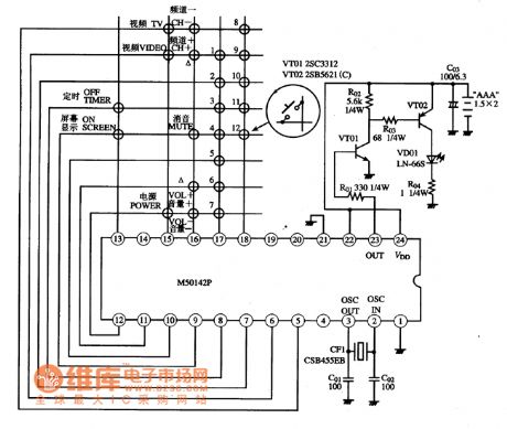
Typical Application Circuit
Typical Application circuit of infrared remote control composed of IM50142P IC is showed as above.Picture:Typical Application Circuit of M50142P IC
Notice:This circuit is the original picture of remote control infrared-emitter so the resistor sign hasn't been modified.
Note:VT01and VT02 are direct coupling system drive circuits.Supply voltage reachs the groundafter it passesinfrared-emitting diode,VD01, and resistance, RO4, when VT02 tube short-circuits.At this time,infrared-emitting diode shines but without any information in infrared light so the remote control is invalid. (View)
View full Circuit Diagram | Comments | Reading(958)
Triangle Wave - Rectangle Wave Generator Circuit
Published:2011/6/4 2:26:00 Author:Michel | Keyword: Triangle Wave, Rectangle Wave, Generator Circuit
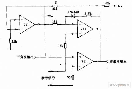
This circuit is composed of three operational amplifiers and its frquency can be altered by changing resistence,R. (View)
View full Circuit Diagram | Comments | Reading(945)
| Pages:19/21 1234567891011121314151617181920Under 20 |
Circuit Categories
power supply circuit
Amplifier Circuit
Basic Circuit
LED and Light Circuit
Sensor Circuit
Signal Processing
Electrical Equipment Circuit
Control Circuit
Remote Control Circuit
A/D-D/A Converter Circuit
Audio Circuit
Measuring and Test Circuit
Communication Circuit
Computer-Related Circuit
555 Circuit
Automotive Circuit
Repairing Circuit