
Filter Circuit
Index 7
RUMBLE_FILTER_2
Published:2009/7/6 8:33:00 Author:May
View full Circuit Diagram | Comments | Reading(640)
FOURTH_ORDER_CHEBYSHEV_BANDPASS_FILTER
Published:2009/7/6 8:32:00 Author:May
View full Circuit Diagram | Comments | Reading(1026)
FOURTH_ORDER_CHEBYSHEV_HIGH_PASS_FILTER
Published:2009/7/6 8:31:00 Author:May
View full Circuit Diagram | Comments | Reading(784)
SIXTH_ORDER_ELLIPTIC_HIGH_PASS_FILTER
Published:2009/7/6 8:30:00 Author:May
View full Circuit Diagram | Comments | Reading(760)
TYPICAL_ACTIVE_BANDPASS_FILTER
Published:2009/7/6 8:27:00 Author:May
View full Circuit Diagram | Comments | Reading(920)
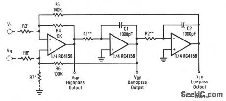
STATE_VARIABLE_FILTER_WITH_MULTIPLE_FILTERING_OUTPUTS
Published:2009/7/6 8:26:00 Author:May
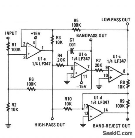
View full Circuit Diagram | Comments | Reading(766)
DYNAMIC_NOISE_FILTER
Published:2009/7/6 8:25:00 Author:May
View full Circuit Diagram | Comments | Reading(831)
SCRATCH_FILTER
Published:2009/7/6 8:23:00 Author:May
View full Circuit Diagram | Comments | Reading(0)
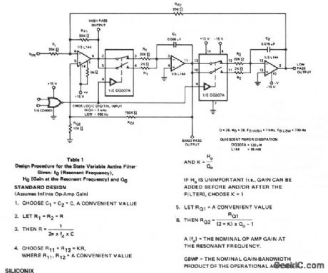
STATE_VARIABLE_ACTIVE_FILTER
Published:2009/7/6 8:22:00 Author:May
A generalized circuit diagram of the two-pole state-variable active filter is shown. The state-variable filter can be inverting or noninverting and can simultaneously provide three outputs: low-pass, bandpass, and high-pass. A notch filter can be realized by adding one summing op amp.
In the state-variable filter circuit, one amplifier performs a summing function and the other two act as integrators. The choice of passive component values is arbitrary, but must be consistent with the amplifier operating range and input signal characteristics. The values shown for C1, C2, R4, R5, and R6 are arbitrary. Preselecting their values will simplify the filter tuning procedures, but other values can be used if necessary. (View)
View full Circuit Diagram | Comments | Reading(2084)
NOISY_SIGNALS_FILTER
Published:2009/7/6 8:19:00 Author:May
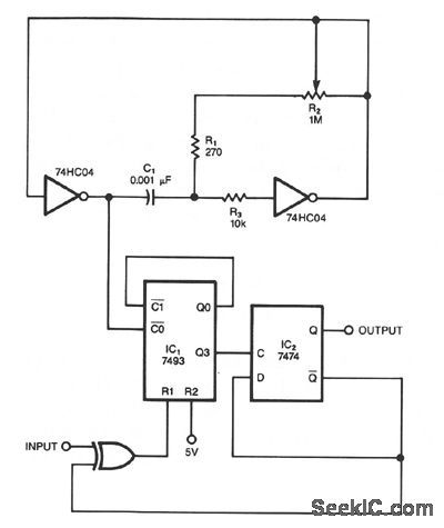
This circuit filters noise, such as glitches and contact bounce, from digital signals. You can easily adjust the circuit for a wide range of noise frequen-cies. The circuit's output changes state only if the input differs from the output long enough for the counter to count eight cycles. If the input changes before the counter reaches its maximum count, the counter resets without clocking the output of flip-flop, IC2. You use R2 to set the frequency of the two-inverter CMOS oscillator, which clocks the counter. Simply adjust the oscillator such that its period is one-eighth that of the noise you want to eliminate. (View)
View full Circuit Diagram | Comments | Reading(765)
SECOND_ORDER_BIQUAD_BANDPASS_FILTER
Published:2009/7/6 8:17:00 Author:May
Note that IQ on each amplifier might be different.AVCL = 10, Q =100,fo=100 Hz. (View)
View full Circuit Diagram | Comments | Reading(695)
VOLTAGE_CONTROLLED_FILTER
Published:2009/7/6 8:13:00 Author:May
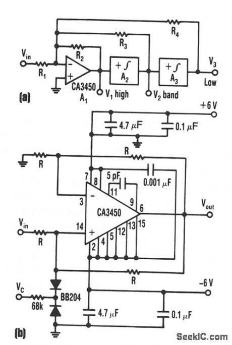
The control voltage VC easily sets the cutoff frequency ωo of this state-variable filter to any desired value, from about 1.7 MHz up to 5 MHz, with a BB 204 varicap and R = 100 KΩ. VC can range from 0 to 28 V. This range changes the capacitance of the varicap from about 4 to 12 pF.The circuit consists of input summing circuit A1 and two noninverting integrators, A2 and A3. Both the integrators and the summing-amplifier cir-cuits use CA3450 op amps. With them, cutoff fre-quencies up to 200 MHz are possible.The circuit's cutoff frequency, it's Q-factor, and gain G are simply:
ωo =2/CR, Q =R3/R4, and G = R4/R1
For a given value for R4, say 10 KΩ,Q depends only upon the resistance of R3. TheQ can be any value, even 100, independently of both ωo and G. Similarly, the gain then depends only on the resistance of R1 and can also be set as high as 100. (View)
View full Circuit Diagram | Comments | Reading(0)
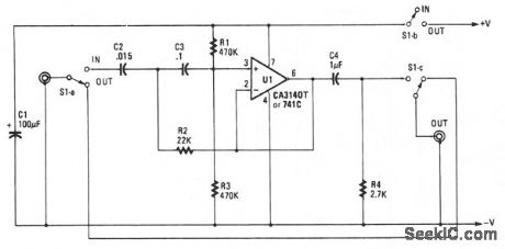
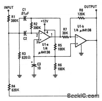
RUMBLE_FILTER_1
Published:2009/7/6 5:51:00 Author:May
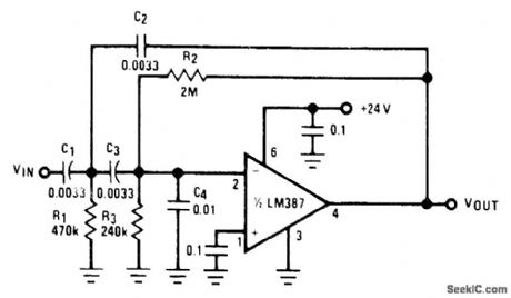
Used to roll off low-frequency noise associated with worn turntable and tape transport mechanisms. Gain is 1. Design procedure is given. For values shown, corner frequency is 50 Hz and slope is -12 dB per octave.- Audio Handbook, National Semi-conductor, Santa Clara, CA, 1977, p 2-49-2-52. (View)
View full Circuit Diagram | Comments | Reading(920)
RUMBLE_FILTER
Published:2009/7/6 5:46:00 Author:May
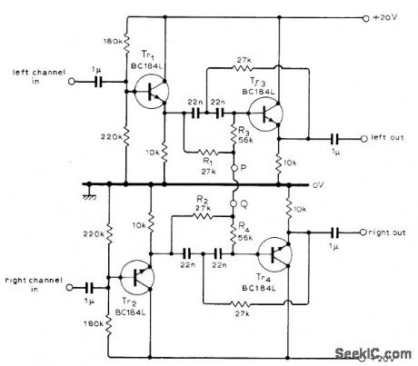
Used when rumble from cheaper turntable or record extends above 100 Hz, causing disconcerting out-of-phase loud-speaker signals, Circuit is based on fact that human ear is not sensitive to directional information below about 400 Hz, making it permissible to remove stereo (L – R) signal at low frequencies and thus remove stereo rumble without losing stereo separation. Emitter-followers feed high-pass filters having 200-Hz breakpoint frequencies and Butterworth characteristics. Attenuation of filter is 12 dB at 100 Hz. Filter circuit can be disabled by placing switch between points P and Q.-M. L. Oldfield, Stereo Rumble Filter, Wireless World, Oct. 1975, p 474. (View)
View full Circuit Diagram | Comments | Reading(6003)
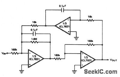
LOW_POWER_ACTIVE_FILTER_WITH_DIGITALLY_SELECTABLE_CENTER_FREQUENCY
Published:2009/7/6 5:34:00 Author:May
The switchable center frequency active filter allows a decade change in center frequency. (View)
View full Circuit Diagram | Comments | Reading(762)
BIQUAD_AUDIO_FILTER
Published:2009/7/6 5:30:00 Author:May
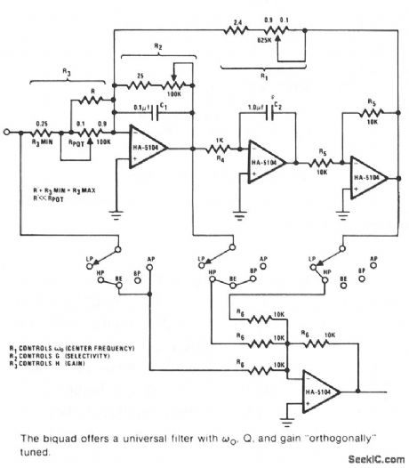
This universal ftlter offers low-pass, high-pass, bandpass, band elimination, and all-pass functions.The Biquad consists of two successive integration stages followed by an inverting stage. The entire group has a feedback loop from the front to the back consisting of R1 which is chiefly responsible for controlling the center frequency, ωo. The first stage of integration is a poor integrator because R2 limits the range of integration. R2 and C form the time constant of the first stage integrator with R3 influencing gain H almost directly. The band-pass function is taken after the ftrst stage with the lowpass function taken after the third stage. The remaining ftlter operations are generated by various combinations of three stages.
The Biquad is orthogonally tuned, meaning that ωo. Q. and gain H can all be independently adjusted. The component values known will allow ωo, to range from 40 Hz to 20 kHz. The other component values give an adequate range of operation to allow for virtually universal filtering in the audio region. ωo Q. and gain H can all be independently adjusted by tuning R1 through R3 in succession. (View)
View full Circuit Diagram | Comments | Reading(1004)
PROGRAMMABLE_ACTIVE_FILTERS
Published:2009/7/6 5:16:00 Author:May
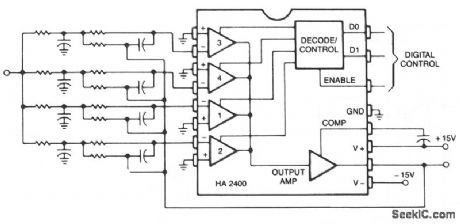
This is a second-order, low-pass filter with programmable cutoff frequency. This circuit should be driven from a low-source impedance since there are paths from the output to the input through the unse-lected networks. Virtually any filter function which can be constructed with a conventional op amp can be made programmable with the HA-2400.
A useful variation would be to wire one channel as a unity gain amplifier, so that one could select the unfiltered signal, or the same signal filtered in various manners. These could be cascaded to provide a wide variety of programmable filter functions. (View)
View full Circuit Diagram | Comments | Reading(1000)
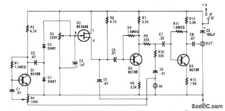
SCRATCH_RUMBLE_FILTER
Published:2009/7/6 1:30:00 Author:May
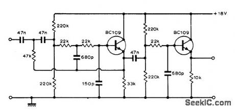
Single active filter provides two widely differing turnover frequencies, as required in audio amplifier used with phonograph. For values shown, insertion loss of filter is -6 dB at 37 Hz and at 23 kHz. Components may be switched to provide different turnover frequencies, but complete removal of filter requires considerably more complicated switching.-P. I. Day, Combined Rumble and Scratch Filter, Wireless World, Dec. 1973, p 606. (View)
View full Circuit Diagram | Comments | Reading(957)
20_Hz_HIGH_PASS_RUMBLE_FILTER
Published:2009/7/6 1:28:00 Author:May
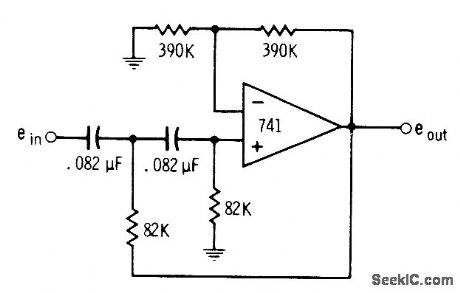
Second-order rumble filter for phonograph amplifier has 1-dB peak and 20-Hz cutoff frequency. Design uses large resistance values to permit use of smaller and lower-cost capacitors.-D. Lancaster, Active-Filter Cookbook, Howard W, Sams, Indianapolis, IN, 1975, p 191-192. (View)
View full Circuit Diagram | Comments | Reading(870)
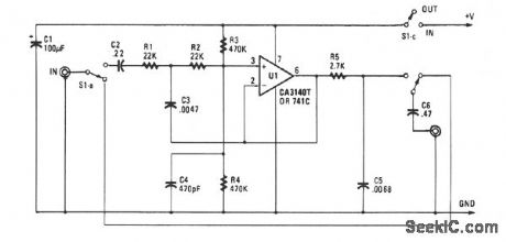
SCRATCH_FILTER
Published:2009/7/6 1:25:00 Author:May
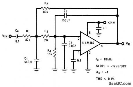
Provides passband gain of 1 and corner frequency of 10 kHz for rolling off excess high-frequency noise appearing as hiss, ticks, and pops from worn records. Design procedure is given.- Audio Handbook, National Semiconductor, Santa Clara, CA, 1977, p 2-49-2-52. (View)
View full Circuit Diagram | Comments | Reading(1595)
| Pages:7/21 1234567891011121314151617181920Under 20 |
Circuit Categories
power supply circuit
Amplifier Circuit
Basic Circuit
LED and Light Circuit
Sensor Circuit
Signal Processing
Electrical Equipment Circuit
Control Circuit
Remote Control Circuit
A/D-D/A Converter Circuit
Audio Circuit
Measuring and Test Circuit
Communication Circuit
Computer-Related Circuit
555 Circuit
Automotive Circuit
Repairing Circuit