
Index 220
CROWBAR
Published:2009/7/20 3:03:00 Author:Jessie
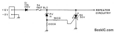
Developed to protect portable repeaters from reverse or excessive voltage when operating on emergency power supply. Zener voltage rating determines maximum voltage that can reach repeater. Diode prevents damage by incorrect polarity. Use fast-blowing fuse.-Circuits, 73Magazine, April 1977, p 164. (View)
View full Circuit Diagram | Comments | Reading(2663)
AM_FM_IF_amplifier_and_detector_using_an_ECG1108_14_pin_DIP
Published:2009/7/20 3:01:00 Author:Jessie
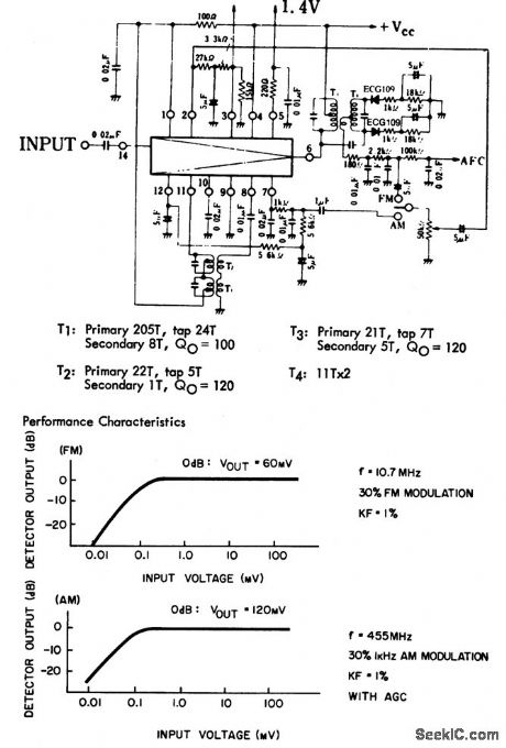
AM/FM IF amplifier and detector using an ECG1108 14-pin DIP. This chip is composed of three major sections. The input signal is fed to pin 14, then amplified by four-transistors. AGC is applied to pin 12. Output from this section is at pin 11. The next section receives its input at pin 8. This section is an AM IF and detector as well as an FM IF and Iimiter. The last section is an audio amplifier with its input at pin 2; output is from pin 3. Typical supply voltage is 5 volts (courtesy GTE Sylvania Incorporated). (View)
View full Circuit Diagram | Comments | Reading(768)
COR_FOR_LINKING
Published:2009/7/20 2:52:00 Author:Jessie
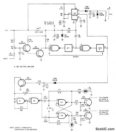
Carrier-operated relay will operate repeater, serve as guard receiver for repeater input channels, and provide loudspeaker muting when no station is being received Simple search-lock feature following CR4 controls two channels, for linking two repeaters or using two-channel drive receiver. Q1 and Q2 are connected as Darlington amplifier for negative-going control signals, as found in vacuum-tube receivers. Dual Schmitt trigger U1 provides positive ON/OFF action. Time-out is controlled by setting of R8 and value of Q3. To monitor repeater or simplex channel for call without listening to other conversations, set timer for about 5 s. When call comes in, first few words will be at normal volume so call can be identified. At time-out, volume will drop to low level. If call is for you, disable COR for normal listening. Search-lock uses single SN7400, with gates G1 and G2 connected as oscillator and gates 63 and 64 as dual D flip-flop. Q3 acts as lock to stop oscillator. With no input carrier, Q3 is off and oscillator makes Q4 and Q5 switch between channels A and B alternately. If signal arrives on one channel, oscillator stops on it and relay closes, bringing repeater transmitter on.-R. C. Heptig and R. D. Shriner, Carrier-Operated Relay for Repeater Linking, Ham Radio, July 1976, p 57-59. (View)
View full Circuit Diagram | Comments | Reading(3328)
MULTIPLEXED_COMMON_CATHODE_LED_DISPLAY_ADC
Published:2009/7/9 22:20:00 Author:May
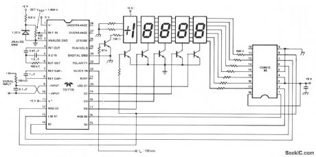
Here, a Teledyne TSC7135 DVM chip is used to drive a multiplexed 5-digit display. A CD4513BE CMOS IC, for common cathode drive, is used as a segment driver selected by pins 17-20 of the DVM chip. The transistors can be any suitable npn type such as 2N3904, etc. (View)
View full Circuit Diagram | Comments | Reading(2095)
LOW_LEVEL_POWER_FET_DRIVER_METHOD
Published:2009/7/9 22:20:00 Author:May
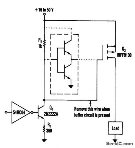
This circuit operates from a 16-to 50-V supply.Adding the buffer circuit(within the dashed lines)offers 100-ns switching times,Otherwise,the circuit switches in 1μs
Q1 and R1 form a switched current source of about 12 mA.The current flows through R2,whichsupplies 12V to the FET.The circuit works well,over a wide range of supply voltages,Furthermore,it switches smoothly in the presence of large ripple and noise on the supply. The switching time(about 1μs)can be reduced considerably by lowering the values of R1 and R2 at the expense of higher power dissipa-tions h the resistors and Q1.Alternatively,a buffer circuit can be added to produce switching times of 100ns without generatmg significant power dissipation. (View)
View full Circuit Diagram | Comments | Reading(774)
NARROW_BAND_FM_RECEIVER
Published:2009/7/9 22:19:00 Author:May

The local oscillator is crystal-controlled and the i-f swing is hardly compressed. The deviation of the transmitted carrier frequency, because of modulation, must therefore be limited to prevent severe distor-tion of the demodulated audio signal. The component values result in an i-f of 4.5 kHz and an i-f bandwidth of 5 kHz. If the i-f is multiplied by N, the values of capacitors C17 and C18 in the all-pass filters, and the values of filter capacitors C7, C8, C10, C11, and C12 must be multiplied by 1/N. For improved i-f selectivity to achieve greater adjacent channel attenuation, second-order networks can be used in place of C10 and C11. (View)
View full Circuit Diagram | Comments | Reading(931)
FM_MPX_SCA_RECEIVER
Published:2009/7/9 22:17:00 Author:May
This receiver is capable of better than 1.5 μt VIHF sensitivity and uses MOSFET front-end circuitry with varactors to eliminate conventional bulky tuning capacitors. It also features high dynamic range, ceramic i-f filters requiring no alignment, and a quadrature-type detector with excellent limiting and AM rejection capability. The receiver operates from nominal 12-V supply. The kit is available from North Coun-try Radio, P.0. Box 53, Wykagyl Station, NY 10804. (View)
View full Circuit Diagram | Comments | Reading(1234)
VOLTAGE_FREEZER
Published:2009/7/9 22:17:00 Author:May
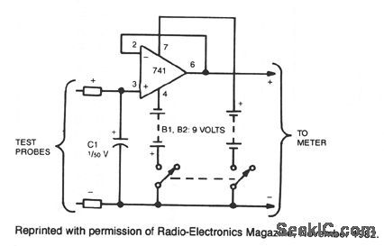
This circuit reads and stores voltages, thus freezing the meter reading even after the probes are removed. The op amp is configured as a unitygain voltage follower, with C1 situated at the input to store the voltage. For better performance, use an LF13741 or a TL081 op amp in place of the 741. These two are JFET devices and offer a much higher input impedance than the 741. (View)
View full Circuit Diagram | Comments | Reading(683)
KEYBOARD_MATRIX_INTERFACE
Published:2009/7/9 22:12:00 Author:May
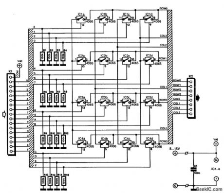
Keyboards can be slotted into two categories, at least as far as the manner that the switches are connected is concerned:those with a common connection and those with the switches arranged in a matrix.
The matrix type has the important advantage that the number of connections is an absolute minimum.Such an arrangement is ideal for ICs; many of these are designed for use with a matrix keyboard.
However, many keyboards are available in job lots, for instance, that apart from a common connection also have a connector for each key. Such keyboards can be connected to ICs that require a matrix type with the aid of a number of electronic switches.
The principle is straightforward: each key of the keyboard controls an electronic switch that is included in a matrix. As an example, the diagram shows a hexadecimal keyboard that is arranged in a 4-x-4 matrix. Each of the electronic switches is held in the open position by a pull-down resistor.
The current drawn by the circuit is very small and is determined mainly by the value of the pull-down resistors and the number of keys being pressed. The CMOS switches draw virtually no current. (View)
View full Circuit Diagram | Comments | Reading(1134)
VERSATILE_ONE_SHOT_CPU_INTERFACE
Published:2009/7/9 22:09:00 Author:May

Process-control applications often require a monostable multivibrator (one-shot) with a pulse width that can be selected on-the-fly.
This circuit uses two CD4051B analog multiplexers to select the required timing components for the multivibrator, and hence, the pulse width. The multiplexers' address input comes from an 8-bit latch. Bit D6 tells the multivibrator whether to trigger on the leading or trailing edge of the trigger input. Bit D7 determines whether the multivibrator should be in a retriggerable or nonretriggerable mode. (View)
View full Circuit Diagram | Comments | Reading(721)
TWO_WIRE_INTERCOM
Published:2009/7/9 22:06:00 Author:May
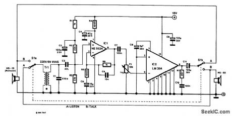
The design consists of an amplifier, a double-pole changeover switch and two loudspeakers:one forthe master station and one for the slave.More than one slave unit can be used,but each reqtures an additional changeover switch.
The power amplifier is a Type LM384,which can provide almost 2 W output at a supply voltage of 15V. Pins 3,4,5,10,11,and 12 are connected to ground and at the same time afford some coolling of thedevice,Because of that,the IC should not be fitted in a socket,but be soldered direct to the circuit board.
The LM384 processes signals with respect to earth so that an asymmetnc supply is sufficient.Theamplification has been set internally to×50(34 dB),The IC’s supply line is decoupled by C9.
To ensure adequate itiput sensitivity,a preamplifier,IC1,IS provided,which has an amplification of 11(21 dB).Because this stage IS intended for speech only, its bandwidth is limited to 160 Hz to 10 kHz.Divider R2/R3 at the input of the op amp is decoupled by C3.
Special loudspeakers that can also serve as microphones are readily available:in the prototype,MS-55units from Monacor were used,but a number of other makes will do Just db well.The bandwidth of the MS-55 (used db loudspeaker)extends from 150 Hz to 20 kHz and (used as a microphone)from 20 Hz to 20kHz,The MS-55 can handle up to 5-W output.To ensure satisfactory operation,particularly as a microphone,the loudspeaker must be fitted In a closed box.
Although it is advantageous for the microphone to have a low internal resistance,it is necessary for a transformer to be used at the input ofthe circuit,This has, however,the advantage that long cables canbe used.The present circuit uses a standard mains transformer instead of a special microphone trans-former. For this purpose,the secondary(6V) winding is connected to the microphone The microphone impedance is thereby magnified from about 8 Ω to around 10 kΩ.The power handling of thetransformer is quite high to ensure that signal losses in the primary winding are kept at a minimum. Capac-itor C1 suppresses HF interference.
If the mains transformer and the microphone transformer are housed in the same enclosure, some trial and error and screening are necessary to eliminate hum. The microphone transformer itself might cause hum in the remainder of the circuit. In that case, the preamp stage must also be screened.
In the prototype, the speech bandwidth was limited from 400 Hz to 4 kHz and this proved perfectly acceptable for good speech transfer. Most of the current drawn by the circuit flows through the power amplifier. At worst, this is 210 mA (680 mA peak), when the amplifier delivers 1.8-W output. The LM384 can deliver a power of up to 5 W. The supply voltage should then be raised to 22 V and a heatsm for the device will be necessary. (View)
View full Circuit Diagram | Comments | Reading(2126)
FM_TUNER
Published:2009/7/9 22:01:00 Author:May

View full Circuit Diagram | Comments | Reading(741)
AM_RADIO
Published:2009/7/9 22:00:00 Author:May
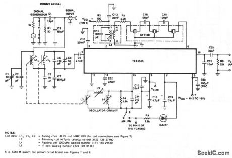
This circuit diagram is for a double-tuned, AM-channel, in-car radio receiver using the TEA5550. (View)
View full Circuit Diagram | Comments | Reading(7560)
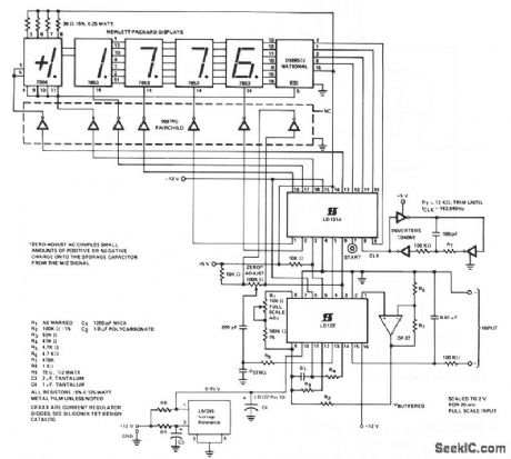
FULL-SCALE_FOUR_DECADE_3_1_2_DIGIT_DVM
Published:2009/7/9 21:59:00 Author:May
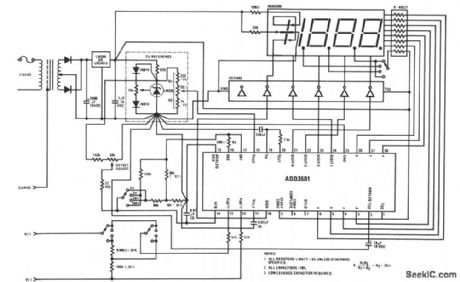
This DVM circuit uses a National ADD3501 DVM chip and an LM336 reference IC to create a simple DVM with relatively few components. When making a single range panel meter, the range switching components can be left out, as required. (View)
View full Circuit Diagram | Comments | Reading(2365)
DIFFERENTIAL_TO_SINGLE_ENDED
Published:2009/7/9 21:55:00 Author:May
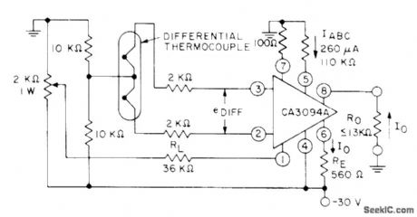
Conversion from differential input signal of thermocouple to single-ended output signal is achieved without feedback by using CA3094A programmable opamp. Output is ±4.7 V at 8.35 mA. Preamp gain is 180. For linear operation, differential input must be equal to or less than ±26 mV,- Circuit Ideas for RCA Linear ICs, RCA Solid State Division, Somerville, NJ, 1977, p 13. (View)
View full Circuit Diagram | Comments | Reading(1026)
4_1_2_DIGIT_DVM
Published:2009/7/9 21:55:00 Author:May
. 1-μV resolution.. Overrange blinking. 0-19.999 mV input voltages. Zero adjust-to-null offset introduced by PC board leakage and the comparator. (View)
View full Circuit Diagram | Comments | Reading(857)
EXTENDED_COMMON_MODE_INSTRUMENT
Published:2009/7/9 21:51:00 Author:May
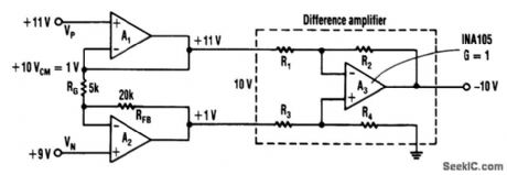
These circuits allow a larger common-mode range than most instrument amplifier inputs can allow. (View)
View full Circuit Diagram | Comments | Reading(678)
VOLTAGE_CONTROLLER_PULSE_WIDTH_GENERATOR
Published:2009/7/9 21:50:00 Author:May

View full Circuit Diagram | Comments | Reading(673)
PICOAMMETER
Published:2009/7/9 21:46:00 Author:May
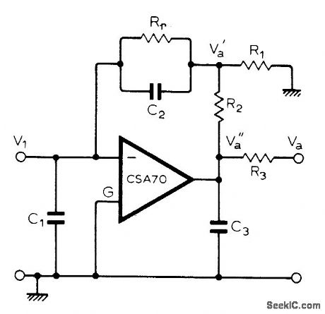
Highly stable circuit uses Valvo CSA70 chopper-stabilized opamp. Required high feedback resistance is provided by R1-R2 in feedback loop. Article gives design equations.Rr' andR2 are 1 megohm, R1 is 10 ohms, and all capacitors are 0.1 μF.-K. Kraus, High-Speed Picoammeter, Wireless World, May 1976,p 78. (View)
View full Circuit Diagram | Comments | Reading(3147)
WIDE_RANGING_PULSER
Published:2009/7/9 21:46:00 Author:May

An output pulse's characteristics depend upon two multivibrator's timing components. IC1's free-running astable-mode frequency sets the pulse's prf, whereas the pulse's width comes from IC2's monostable operation. (View)
View full Circuit Diagram | Comments | Reading(681)
| Pages:220/471 At 20201202203204205206207208209210211212213214215216217218219220Under 20 |
Circuit Categories
power supply circuit
Amplifier Circuit
Basic Circuit
LED and Light Circuit
Sensor Circuit
Signal Processing
Electrical Equipment Circuit
Control Circuit
Remote Control Circuit
A/D-D/A Converter Circuit
Audio Circuit
Measuring and Test Circuit
Communication Circuit
Computer-Related Circuit
555 Circuit
Automotive Circuit
Repairing Circuit