
Index 212
BIKE_SPEEDOMETER
Published:2009/7/10 2:18:00 Author:May
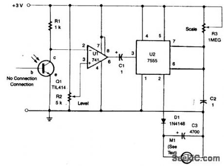
A TIL414 photo transistor senses reflection from a spoke-mounted reflector. This generates a pulse and sends it to U1 and U2, a monostable multi ibrator, which drives meter M1. (View)
View full Circuit Diagram | Comments | Reading(1169)
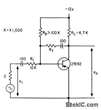
100_MEG_INPUT_IMPEDANCE
Published:2009/7/10 2:17:00 Author:May
Variation of Darlington connection gives low-noise amplifier with high input impedance. Thermal and shot noise are much lower than ficker, leakage, and surface noise.-I. Levine, High Input Impedance Transistor Circuits, Fleetronics, 33:36, p 50-52. (View)
View full Circuit Diagram | Comments | Reading(751)
ELECTRONIC_BAGPIPE
Published:2009/7/10 2:17:00 Author:May
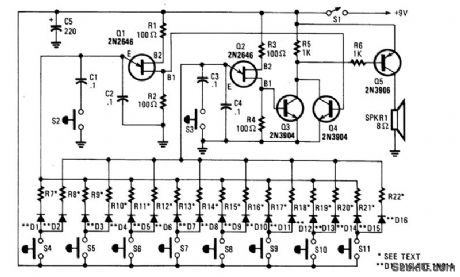
The electronic bagpipe mimics the sound of real instruments. This circuit uses two UJT oscillators and an amplifier (Q3, Q4, and Q5). R7 through R22 are selected for tonal range desired (typically 3300 Ω). Each key selects resistors for the two oscillator circuits Q1 and Q2. S2 and S3 vary the tonal range of S4 through S11. (View)
View full Circuit Diagram | Comments | Reading(0)
MOS_FET_WITH_NPN
Published:2009/7/10 2:16:00 Author:May
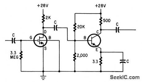
FET input stage serves as high-to-low impedance transformer for power transistor and gives very high power gain.-D. M. Griswold, Understdnding and Using the MOS FET, Electronics, 37:31, p 66-70. (View)
View full Circuit Diagram | Comments | Reading(851)
BROADBAND_AC_ACTIVE_RECTIFIER
Published:2009/7/10 2:16:00 Author:May
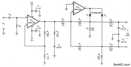
This circuit converts sine waves of up to 1-V rms into an equivalent dc level. It should prove useful as an ac broadband voltmeter. IC1 is an input amplifier that converts level from rms to an equivalent dc level and feeds ICB1. R3 and C3 are stabilizing components. IC2 acts as a full-wave rectifier. R6, R5, and D1 rectify positive levels, R7, R8, and D2 negative-going signals. R9, R10, C4, and C5 are low-pass filters.The output can feed a DVM or another meter. (View)
View full Circuit Diagram | Comments | Reading(1035)
DIRECTLY_COUPLED_MOS_FET
Published:2009/7/10 2:16:00 Author:May
Eliminates coupling capacitors but requires additional bias supply.-D. M. Griswold, Understanding and Using the MOS FET, Electronics, 37:31, p 66-70. (View)
View full Circuit Diagram | Comments | Reading(569)
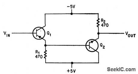
SIMPLE_PHOTOELECTRIC_LIGHT_CONTROLLER
Published:2009/7/10 2:15:00 Author:May
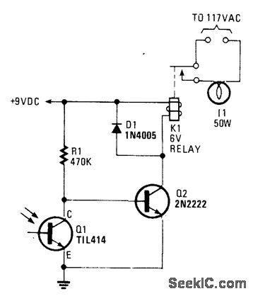
A phototransistor senses daylight. At dusk, it ceases to conduct and R1 biases Q2, activates K1, and switches on the light. At dawn, Q1 starts to conduct, and Q2 is cut off. K1 drops out and the light goes out. (View)
View full Circuit Diagram | Comments | Reading(772)
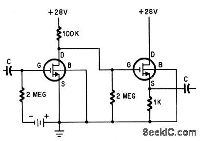
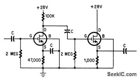
VOLTAGE_CONTROLLED_ATTENUATOR
Published:2009/7/10 2:15:00 Author:May
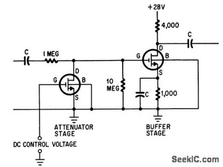
Can attenuate input signals 70 db when mos let is followed by high-impedance load such as common-source mos fet amplifier.-D. M. Gris-wold, Understanding and Using the MOS FET, Electronics, 37:31, p 66-70. (View)
View full Circuit Diagram | Comments | Reading(0)
NONLINEAR_FEEDBACK_LOOP
Published:2009/7/10 2:14:00 Author:May
Type WE41A copper-oxide varistor for Rf in feedback loop gives radically different voltage-gain charctcteristic than silicon diode for Rf, but both give exponential response and increase dynamic range.-J. C. Looney, Designing Amplifiers with Nonlinear Feedback, Electronics, 34:13, p 46-49. (View)
View full Circuit Diagram | Comments | Reading(626)
LOW_SUPPLY_VOLTAGE_VHF
Published:2009/7/10 2:13:00 Author:May
Good high-frequency parameters of epitaxial mesa transistor give high gain and efficiency at supply voltage of only 12 v. Output is 0.5 w ct 70 Mc.-D. Hall, Using Epitaxial Transistors in Switching and R-F Circuits, Electronics, 34:13, p 52-53. (View)
View full Circuit Diagram | Comments | Reading(502)
MICROPOWER_CLOCK
Published:2009/7/10 2:13:00 Author:May
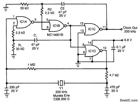
Although ceramic resonators are a good choice for low-power, low-frequency clock sources (if you can stand their 30-ppm temperature coefflcient), they have troublesome, spurious-resonance modes. This circuit rejects all but the resonator's fundamental mode. This clock circuit works from -40 to +80℃ and consumes only 2.8 mW.
The rising edge of resonator Y1 toggles IC1A low. ac-coupled positive feedback from IC1D via C1 and R1 immediately confirms this state change at IC1B so that Miller loading, harmonic components, or below-minimum rise times at IC1A cannot force IC1C to relapse to its previous state. This tactic also applies to resonator Y1's falling edge because IC1C, via CZ agd R2, holds ICIB high.
Choose time constants R1C1, and R2C2 to be equal and ranging from 60 to 75% of one-half of the clock's period. Ceramic capacitors (10% tolerance) with X7R dielectric work well. With these time constants, the logic will be locked and unavailable to the ceramic resonator until just before it executes a legitimate transition. IC1D and IC1C are in parallel to isolate the resonator from external loads and, more importantly, from C2. (View)
View full Circuit Diagram | Comments | Reading(0)
HOLD_CURRENT_LIMITER
Published:2009/7/10 2:12:00 Author:May
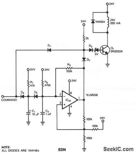
In many applications, a solenoid driver must ftrst briefly supply a large amount of pull-in current, which quickly actuates the solenoid. Thereafter, the driver must supply a much lower holding current to avoid burning the solenoid out. To avoid using the customary, cumbersome, large capacitors or power-wasting resistors, you can use the switch technique.As long as the input to the circuit is low, diode D1 holds Q1 off; a low input also prevents the op-amp circuit from oscillating. When the input reaches 24 V, Q1 switches on and pulls in the solenoid. Concurrently, D4 is back-biased, and C1 begins charging up. When C1 charges up, the op-amp circuit begins to oscillate, switching Q1 on and off.The time constant defmed by R1 and C1 determines the length of the period during which the solenoid receives full power. R3 and C2 set the oscillator's frequency, and R2 sets the oscillator's duty cycle. The hold current is directly proportional to the duty cycle. For the components shown, the full-power period is 300 ms, the oscillator's frequency is 3 kHz, and its duty cycle is 50%. (View)
View full Circuit Diagram | Comments | Reading(812)
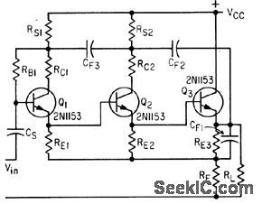
BROADBAND_IMPEDANCE_TRANSFORMER
Published:2009/7/10 2:10:00 Author:May
Darlington circuit gives unity gain from d-c up to several Mc, using any complementary pair of transistors having sufncienlly high gain and cutoff frequency.-I. Ingemarsson, Darlington Maintains Constant Unity Gain, Electronics, 38:22, p 69.
(View)
View full Circuit Diagram | Comments | Reading(690)
LIGHT_PROBE
Published:2009/7/10 2:10:00 Author:May
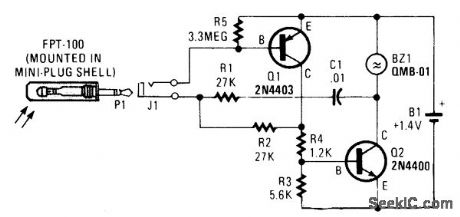
Originally designed as an aid for blind people, this probe was used as a light detector in order to tell if a device or room lights are on or off. (View)
View full Circuit Diagram | Comments | Reading(864)
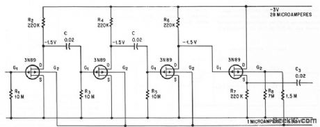
TWO_STAGE_MOS_FET
Published:2009/7/10 2:09:00 Author:May
Pain of 3N98 transistors give voltage gain of 10 with low output impedance.-D. M. Griswold, Understanding and Using the MOS FET, Electronics, 37:31, p 66-70. (View)
View full Circuit Diagram | Comments | Reading(857)
ELEKTOR_ELECTRONICS
Published:2009/7/10 2:08:00 Author:May
The control of this compressor is based on the dependence of the dynamic resistance of a diode on the current flowing through it. The heart of the present circuit is the diode bridge (D1 through D4), which behaves as a variable resistance controlled by the current flowing in T1.The input signal is applied to preamplifier state A1 via low-pass filter R1/C1 that removes any HF noise from the input.Switch S1 in the feedback loop of A1 sets the amplification to 1 (position A), 6 (C) or 11 (B). The amplified signal is applied directly to the diode bridge via R12 and C5, and inverted via inverter A2, capacitor C6 and resistor R13.The two signals are summed by the bridge, amplified (in A3), then split again into two, one of which is inverted by A4. The positive half cycles of the two signals are used to switch on T2 and T3, respectively. Capacitor C11 is then charged via R12. When the potential across this capacitor reaches a certain level, T1 is also switched on, after which a control current flows through the bridge via R21. This current lowers the resistance of the bridge so that the signal is attenuated (compressed). At the same time, the LED lights to indicate that the signal is being compressed. Capacitor C12 prevents any dc voltage from reaching the output.The output signal is taken from the wiper of P1. Low-pass section R20/C13 limits its bandwidth to 12 kHz. Switch S2 enables the selection of various decay times from C11. The values shown in the diagram are the most useful. Nevertheless, these values are subjective and can be altered to personal taste and requirements.
(View)
View full Circuit Diagram | Comments | Reading(2308)
PRECISION_FULL_WAVE_ac_dc_CONVERTER
Published:2009/7/10 2:08:00 Author:May
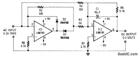
A dc level is produced that corresponds to the ac input rms value (if sine wave). R1/C5 set the gain of IC2 to 1.11. This factor is the average-to-rms conversion factor. IC1 and IC2 act as a full-wave rectifier circuit, with D1 and D2. (View)
View full Circuit Diagram | Comments | Reading(2098)
FET_MICROPOWER
Published:2009/7/10 2:08:00 Author:May
Voltage gain is 60 db from 1 cps to 30 kc, with O.5 v rms maximum output voltage, for power drain under l00 microwatts. First three transistors should be matched.-J. S. Sherwin, An FET Micropower Amplifier, Electtonics, 37:31, p 74-75. (View)
View full Circuit Diagram | Comments | Reading(600)
SINE_WAVE_SQUARE_WAVE_CONVERTER
Published:2009/7/10 2:07:00 Author:May
An op amp used as a comparator produces a 10-V p-p square-wave output with 100-mV input, to 15 kHz. Adjust R5 for symmetry of square wave at low input levels. (View)
View full Circuit Diagram | Comments | Reading(3172)
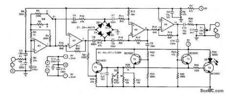
DIGITAL_TACHOMETER_CIRCUITRY
Published:2009/7/10 2:06:00 Author:May
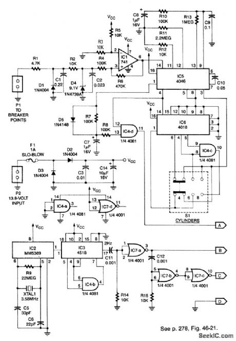
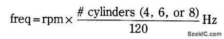
This system can be used with 4-, 6-, or 8-cylinder automobiles. The timebase formed by IC5 is an oscillator that drives counter IC6, which divides by 6, 4, or 3 for 4-, 6-, or 8-cylinder engines, respectively.S1 selects this number IC5 produces a signal that is phaselocked to this multiple of the ignition system frequency, which in turn depends on engine speed.
ICl conditions the ianition input at PI to feed IC5. The output of IC4D, which is the same frequency as the VC0 in IC5, is fed to the frequency display.
IC2 generates a 60-Hz sianal using a 3.58-MHz reference. IC3 and IC4B divide this by 30 to produce 2Hz. IC7B/IC7C and C12/R15 produce a delayed 2-Hz signal. These sianals are fed to the counter circuit. (View)
View full Circuit Diagram | Comments | Reading(1598)
| Pages:212/471 At 20201202203204205206207208209210211212213214215216217218219220Under 20 |
Circuit Categories
power supply circuit
Amplifier Circuit
Basic Circuit
LED and Light Circuit
Sensor Circuit
Signal Processing
Electrical Equipment Circuit
Control Circuit
Remote Control Circuit
A/D-D/A Converter Circuit
Audio Circuit
Measuring and Test Circuit
Communication Circuit
Computer-Related Circuit
555 Circuit
Automotive Circuit
Repairing Circuit