
Index 210
TIME_DELAY_PHOTO_FLASH_TRIGGER
Published:2009/7/10 3:39:00 Author:May
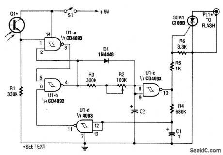
Q1 is a phototransistor that is normally illuminated by a beam of light. When the beam is intercoupled, pin 1 of U1A goes high, and forces pin4 U2B low. Then, C2 discharges through R2 and R3. After a certain time delay, pin 10 U1C goes high, triggers SCR1, and sets off the flash. R4/C1 charges, causes U1D out-put to go low after about 1/2 second, and resets U1A and U1B to the initial state. This delay prevents accidental double flash exposure. (View)
View full Circuit Diagram | Comments | Reading(867)
CALIBRATED_TACHOMETER
Published:2009/7/10 3:36:00 Author:May

Here is a simple tachometer circuit for use with a hand-held DVM or portable chart recorder. A novel feature is that the source frequency pulse/rev rate can be directly set on a ten-turn potentiometer to provide a convenient calibration of one V per 1000 rev/min. This is particularly useful when measuring a shaft or engine speed by sensing gear teeth.The circuit uses an LM2917 IC which is specifically designed for tachometer applications. The ten-turn potentiometer, which provides the pulse/rev setting, is suitably conftgured in the output amplifter feedback path. The pulse/rev range is 100 to 1100, so the potentiometer dial mechanism should be set to start at 100 to provide direct calibration.The IC's internal 7.5-V zener provides stable operation from a 9-V battery. The tachometer accepts an input signal between 50 mv and 20 V rms and has an upper speed limit of 6000 rev/min with the compo-nent values shown. (View)
View full Circuit Diagram | Comments | Reading(2740)
SYNCHRONOUS_SYSTEM
Published:2009/7/10 3:32:00 Author:May
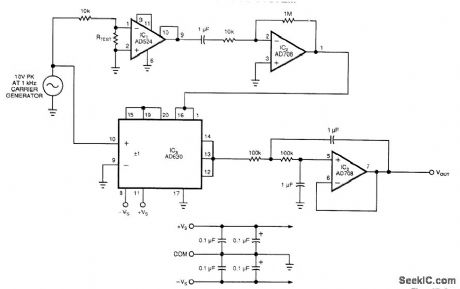

The circuit uses a synchronous-detection scheme to measure low-level resistances. Other low-resis-tance-measuring circuits sometimes inject unacceptable large currents into the system-under-test.This circuit synchronously demodulates the voltage drop across the system-under-test and can hence use extremely low currents while measuring resistance.The 10-V (pk), 1-kHz carrier generator injects a 1-mA reference current into unknown resistor, RTEST. Instrument amplifier IC1 and precision op amp IC2A amplify the voltage across RTEST by a gain of 100000. Synchronous detector IC3 demodulates this voltage, then op amp IC2B acts a low-pass filter on the demodulated voltage. The low-pass filtering will attenuate all uncorrelated disturbances (such as noise, drift, or offsets), while passing a dc voltage that is proportional to the unknown resistance.
The relationship between the output voltage and the unknown resistance is:
(View)
View full Circuit Diagram | Comments | Reading(946)
LOW_FREQUENCY_TACHOMETER
Published:2009/7/10 3:30:00 Author:May
This tachometer lets you measure heartbeats, respiratory rates, and other low-frequency events that recur at intervals of 0.33 to 40.96 seconds. The circuit senses the period of fIN, computes the equivalent pulses per minute, and updates the LCD accordingly. Although the decimal readout equals 60 fIN, the circuit doesn't actually produce a frequency of 60 fIN. The computation involves counting and comparison techniques and takes 0.33 seconds. (View)
View full Circuit Diagram | Comments | Reading(873)
ON_OFF_INVERTERS
Published:2009/7/10 3:27:00 Author:May
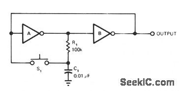
Each time the switch closes, the voltage on C1 causes inverter A to change state, with positive feedback from inverter B. Resistor R1 delays the charging and discharging of C1, making the circuit virtually immune to contact bounce. The circuit works with either CMOS or TTL gates. The values of R1 and C1 are not critical and can be increased for greater contact bounce protection, if needed.Recommended ranges are 10 K to 1 MΩ for R1, and 0.01 to 1.0 μF for C1. (View)
View full Circuit Diagram | Comments | Reading(827)
BIKE_SPEEDOMETER_1
Published:2009/7/10 3:21:00 Author:May
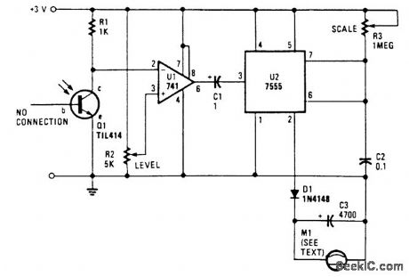
A TIL414 photo transistor senses reflection from a spoke-mounted reflector, generates a pulse, and sends it to U1 and U2, a monostable multivibrator, which drives meter M1. (View)
View full Circuit Diagram | Comments | Reading(1091)
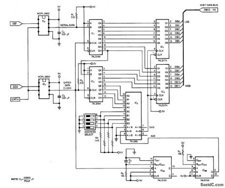
ANALOG_DATA_SIGNALS_ISOLATER
Published:2009/7/10 3:13:00 Author:May
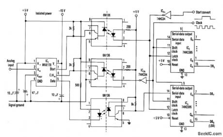
By converting analog data to digital and usmg optocouplers,this circuit can be used to transmit analogsignals across barriers,such as voltage levels,different ground systems,etc. (View)
View full Circuit Diagram | Comments | Reading(1534)
DIODE_MATCHING_CIRCUIT
Published:2009/7/10 3:11:00 Author:May
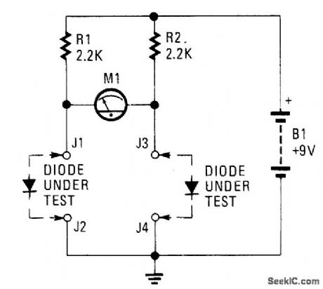


This circuit can be used to match diodes for use in circuits where such a balance is necessary (a balanced modulator, for instance).The diode matching circuit will indicate the forward-voltage drop of the two diodes in millivolts. (View)
View full Circuit Diagram | Comments | Reading(885)
LOW_FREQUENCY_PRESCALER
Published:2009/7/10 3:10:00 Author:May
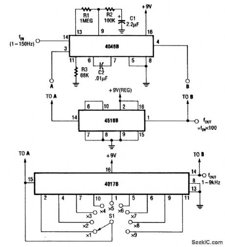
For multiplying frequencies in the 1-to 150-Hz range, this circuit uses a 4046B and a + 100 prescaler. The VCO output is phaselocked to the low-frequency input. This simplifies use of a frequency counter to measure LF signal frequencies.
By using a 4017B and a 1-kHz fIN, the circuit can be used as a 1-to 9-kHz frequency synthesizer or as a x 10 frequency multiplier. (View)
View full Circuit Diagram | Comments | Reading(997)
ANALOG_TACHOMETER_READOUT
Published:2009/7/10 3:10:00 Author:May
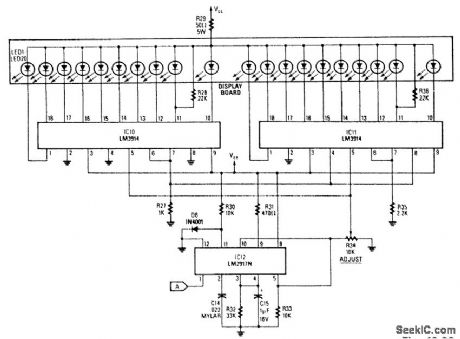
The analog display consists of a frequency/voltage converter (IC12) and bar-graph segment drivers IC10 and IC11. R34 is the calibration adjustment and is set so that an engine rpm of 5000 to 7000 rpm lights the first LED (redline value). (View)
View full Circuit Diagram | Comments | Reading(3032)
DATA_ACQUISITION_SYSTEM_Ⅱ
Published:2009/7/10 3:08:00 Author:May
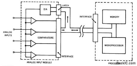
In this circuit, an HA-4900 series comparator is used in conjunction with a D/A converter to form a simple, versatile, multichannel analog input for a data acquisition system. The processor first sends an address to the D/A, then the processor reads the digital word generated by the comparator outputs. lb perform a simple comparison, the processor sets the D/A to a given reference level, then examines one or more comparator outputs to determine if the inputs are above or below the reference. A window comparison consists of two such cycles with two reference levels set by the D/A. 0ne way to digitize the inputs would be for the processor to increment the D/A in steps. The DiA address, as each comparator switches, is the digitized level of the input. While stairstepping, the D/A is slower than successive approximation; all chan-nels are digitized during one staircase ramp. (View)
View full Circuit Diagram | Comments | Reading(548)
DATA_ACQUISITION_SYSTEM_I
Published:2009/7/10 3:07:00 Author:May
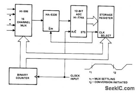
The Hl-506 multiplexer is used as an analog input selector, controlled by a binary counter to address the appropriate channel. The HA-5330 is a high-speed sample and hold. The sample/hold control is tied to the status (STS) output of the HI-774A; whenever a conversion is in process, the S/H is in the hold mode. A conversion is initiated when the clock input becomes low; when the clock becomes high, the mux address changes. The mux will be acquiring the next channel while the ADO is converting the present input, held by the SiH. The clock low time should be between 225 ns and 6.5 ps, with the period greater than 8.5 μs.
With this timing, T/C will be high at the end of a conversion, so the output data will be valid ~ 100 ns before STS goes low. This allows STS to clock the data into the storage register. The register address will be offset by one; if this is a problem, a 4-bit latch can be added to the input of the storage register. With a 100-kHz clock rate, each channel will be read every 160 μs. (View)
View full Circuit Diagram | Comments | Reading(655)
CAPACITOR_ESR_MEASURER
Published:2009/7/10 3:07:00 Author:May
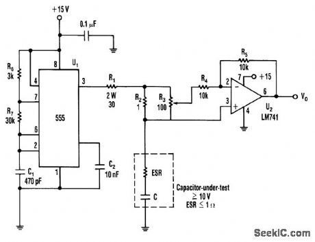
The equivalent series resistance (ESR) of a capacitor can be measured using this circuit and an ac voltmeter. U1 functions as a 50-kHz square-wave generator. It drives a current waveform of about ±180mA in the capacitor-under-test, through R1 and R2. When R3 is adjusted to the proper value, the voltage drop across the equivalent series resistor is precisely nulled by the inverting amplifier (U2). Thus, VO is the pure capacitor voltage which is the minimum voltage that can be produced at VO.
To make an ac voltage measurement, adjust R3 until VO is minimized. Then, note the position of the potentiometer and multiply it by the value of R2, 1Ω in this case. That product equals the capacitor's ESR. The capacitor is biased at about 7.5 V. Lower-voltage capacitors won't work with this circuit. By changing the value of R2, other ranges of ESR can be measured. However, for small R2 values, the current level should be increased to keep a reasonable voltage across R2. This requires some sort of buffer. The circuit is intended for capacitors greater than 100μF. The ripple voltage gets large for smaller values and accuracy decreases. (View)
View full Circuit Diagram | Comments | Reading(1152)
3_WIRE_RECEIVER_MESSAGE_DEMUXER
Published:2009/7/10 3:05:00 Author:May
This 3-wire receiver checks the first four data bits of 16 received bits against a preset address. If the two match, the remaining 12 bits are latched into two 6-bit flip-flop registers. Either CMOS or TTL logic families can be used in the design. (View)
View full Circuit Diagram | Comments | Reading(624)
ECONOMICAL_CRYSTAL_TIME_BASE
Published:2009/7/10 3:01:00 Author:May
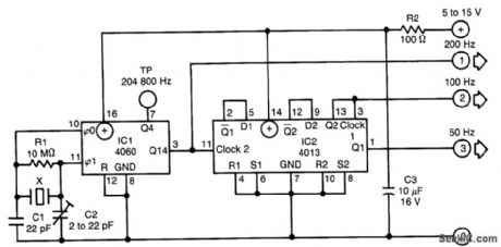
The above time base circuit will provide 50-, 100-, or 200-Hz signals from an inexpensive crystal cut for 3.2768MHz, a common crystal used for microprocesser works. It requires a power supply of 5 to 15 V at 0.05 to 2.5 mA. (View)
View full Circuit Diagram | Comments | Reading(1572)
SINGLE_CHIP_CHIME
Published:2009/7/10 3:00:00 Author:May
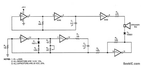
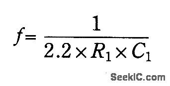
This circuit uses only one IC, produces a pleasant tone, and sports a single control for adjusting the tone's chiming rate. IC1A and IC1B form an astable multi ibrator, which produces the circuit's basic tone. The multivibrator's frequency is:The component values produce a 668-Hz tone. IC1C buffers the multivibrator's output to the 8- Ω speaker. Current-limiting resistor R2, determines the speaker's volume. R2 minimum value is 220 Ω. IC1D and IC1E form an asymmetric, astable multivibrator, which adds a chime effect to the circuit's basic tone. The chime effect's frequency is:R7 gives this rate multivibrator a slowly varying output signal to produce a pleasant decay for the chime effect. IC1F is an inverting amplifier for the chime multivibrator. (View)
View full Circuit Diagram | Comments | Reading(788)
SIMPLE_ELECTROMETER
Published:2009/7/10 2:59:00 Author:May
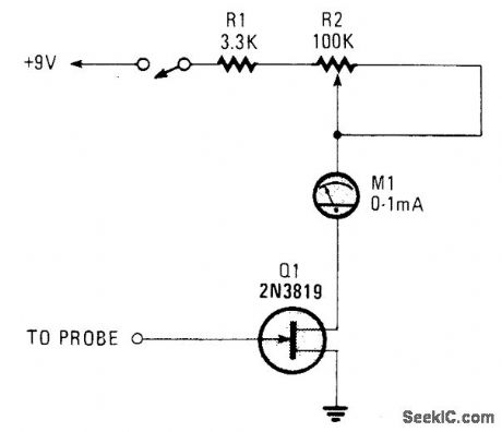
This electrometer is useful as a relative indicator of static charges or as an electric fteld in a chargefree environmen.An induced negative charge on the probe will reduce drain current toward zero. (View)
View full Circuit Diagram | Comments | Reading(1608)
ELECTROLYTIC_CAPACITOR_REFORMING_CIRCUIT
Published:2009/7/10 2:45:00 Author:May


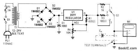
Sometimes electrolytic capacitors that are stored for some time will exhibit high leakage currents.Before placing these in service, the capacitors might need to be reformed. This power supply can be used for reforming. Adjust R4 for the capacitor's rated voltage and set S2 in position 1. When M1 indicates the rated voltage, reforming is complete. For large capacitors, use position 2, and then position 3 after reform-ing starts. T1 can be any transformer with a rating of 12 to 24 Vac at about 1A. (View)
View full Circuit Diagram | Comments | Reading(2577)
STATIC_DETECTOR
Published:2009/7/10 2:43:00 Author:May
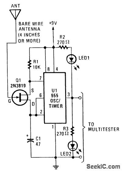
This circuit detects the presence of electrostatic fields by using an FET to alter the flash rate of two LEDs. The FET is installed in the timing circuit and causes a change in the flash rate of the two LEDs. (View)
View full Circuit Diagram | Comments | Reading(2990)
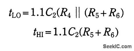
NEARLY_50_DUTY_CYCLE_MULTIVIBRATOR
Published:2009/7/10 2:37:00 Author:May
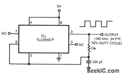
Three factors contribute to the output symmetry. The capacitor charges and discharges through the same external resistor. An internal resistive divider sets accurate switching thresholds within the chip, the bipolar types use dividers, as well.Most importantly, 101's CMOS output stage switches fully between ground and VCC, avoiding the errors from asymmetry that are often found in a TTL timer's output. The IC's internal switching-threshold tolerances can cause a deviation of several percent from the desired 50% duty cycle. To meet a tighter specification, you might have to select from a group of ICs. (View)
View full Circuit Diagram | Comments | Reading(632)
| Pages:210/471 At 20201202203204205206207208209210211212213214215216217218219220Under 20 |
Circuit Categories
power supply circuit
Amplifier Circuit
Basic Circuit
LED and Light Circuit
Sensor Circuit
Signal Processing
Electrical Equipment Circuit
Control Circuit
Remote Control Circuit
A/D-D/A Converter Circuit
Audio Circuit
Measuring and Test Circuit
Communication Circuit
Computer-Related Circuit
555 Circuit
Automotive Circuit
Repairing Circuit