
Index 246
420_450_MHz_100_W_LINEAR
Published:2009/7/7 4:50:00 Author:May
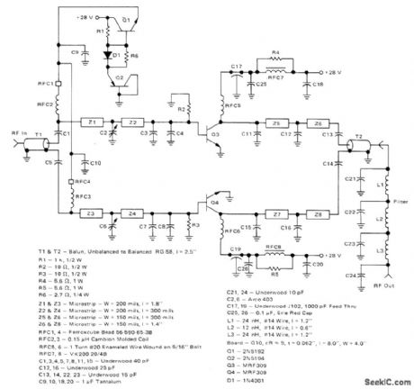
Two Motorola 3-inch lengths and prepare MRF309 transistors in pusffipull require only 16 and W drive to deliver 100 W for transmitter applications. Circuit provides 8 dB of power gain at efficiency greater than 40% when operating from 28-V supply. Harmonic suppression inherent in push-pull operation is enhanced by seven-element low-pass filter at output. Q1and Q2 are bias resistors and must be insulated from heatsink with mica washers. T1 and T2 are transformers constructed from RG58 coax. Use 1/4 inch at each end to give total transformer length of 21h inches.H. Swanson and B. Tekniepe, A 100-Watt PEP420-450 MHz Push-Pull Linear Amplifier, Motorola, Phoenix, AZ, 1978, EB-67. (View)
View full Circuit Diagram | Comments | Reading(787)
2_MHz_MASTER_CLOCK
Published:2009/7/7 4:47:00 Author:May
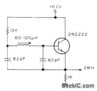


Developed for use with Geneml lnstruments AY-3-8500-1TV game chip,which contains dividers that deliver required 60-Hz vertical and 15.75-kHz horizontal sync signals for video signal going to TV set. Coil is Miller 9055 miniature slugtuned. Article gives other circuits for game.-S.Ciarcia,Hey,Look What My Daddy Builtl,73 Magazine,0ct.1976,p 104-108 (View)
View full Circuit Diagram | Comments | Reading(1082)
DIFFERENTIAL_TO_ABSOLUTE_VALUE
Published:2009/7/7 4:47:00 Author:May
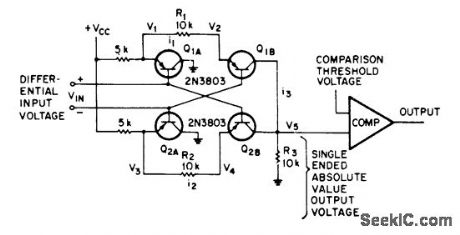
Used in comparing differential level to threshold level with good common-mode rejection. Input impedance is maintained high to avoid over loading differential input. Output voltage re-mains positive when input polarity is re-versed.-R. L. Wiker, Differential to Absolute Value Converter, EEE Magazine, Jan. 1971, p 65. (View)
View full Circuit Diagram | Comments | Reading(813)
OPTICALLY_COUPLED_V_F
Published:2009/7/7 4:44:00 Author:May
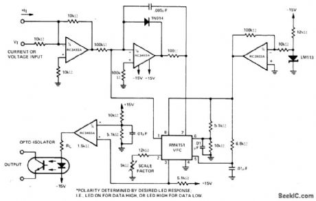
Input voltage range of 0-10 V is converted to proportional frequency at output of optoisolator with high linearitv bv RM4151 converter used in combination with RC3403A quad opamp that provides. functions of inverter, integrator, regulator, and LED driver.-"Linear Integrated circuit Data Book,"Raytheon Semiconductor Division, Mountain View,CA,1978, p 7-40-7-41. (View)
View full Circuit Diagram | Comments | Reading(677)
7_SEGMENT_TO_BCD_1
Published:2009/7/7 4:41:00 Author:May

Arrangement uses SN7448 BCD to 7-segment decoder IC4.as lookup table for inverse decoding technique,When desired 7-segment code is applied to input of decoder and does not match output code from IC4.gate IC3,output is logic 1 This allows pulses from clock to advance BCD counter IC5,until its decoded state from IC4 matches that of input code,With coincidence,output of IC3 goes low, holding proper BCD code in IC5,and indicating by means of IC6b that BCD information is ready With 100-kHz clock,correct code is available for at least 90% of digit display time.-J.P.Cater,7-Segment to BCD Decoder,EDN Magazine,Feb.20,1973,p 92-93. (View)
View full Circuit Diagram | Comments | Reading(3453)
SQUARE_TO_SlNE
Published:2009/7/7 4:37:00 Author:May
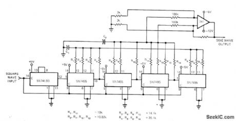
Transversal digital filter suppresses harmonics present on input square wave, to give pure sine wave. Resistors weight data as it passes through 16-bit shift register, so sine wave is sampled at 16 times its frequency and theoretically has no harmonics below the 16th. Simple RC filter removes remaining harmonics. Input is clock whose repetition rate is 16 times desired frequency. SN74L93 4-bit ripple counter divides this down to provide square wave of desired frequency. Square wave is sampled 16 times per cycle and shifted down SN7495 16-bit shift register. C1 and C2 are selected to eliminate higher harmonics. Sine-wave output has harmonic distortion of less than -50 dB.-L. J. Mandell, Sine-Wave
Synthesizer Has Low Harmonic Distortion, EDN Magazine, Aug. 15, 1972, p 52. (View)
View full Circuit Diagram | Comments | Reading(1385)
VOLTAGE_TO_PULSE_DURATION
Published:2009/7/7 4:31:00 Author:May

Optical Electronics 9829 opamps are used as fast comparators and 9718 FET opamp as fast integrator to give high precision at high speed for converting analog voltage to pulse duration for such applications as A/D conversion, delta code generation, motor speed control, and pulse-duration modulation. Output pulse durations can be as short as 1 μs. Conversion linearity is better than 0.1%. Minimum pulse duration is 100 ns, and maximum dynamic range is 40 dB. Reference voltages are determined by×input; if×is 3 V, reference voltages differ by 6 V. Two 9829 opamps present reference voltages to two com-parator opamps. Fifth 9829 sums comparator outputs and gives positive output.- Voltage to Pulse Width Converter, Optical Electronics, Tucson,AZ, Application Tip 10230. (View)
View full Circuit Diagram | Comments | Reading(1638)
80_METER_CWFOR_0RP
Published:2009/7/7 4:30:00 Author:May
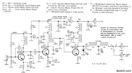
Low-powertransmit-tercan be mounted on small can for operation from separate 12-V supply. Zener D1 protects 03 by clamping on RF voltage peaks in excess of 36 V, Output tank of 03 gives satisfactory operation from 3.5 to 3.75 MHz without tuning.-D. DeMaw, Build This Sardine Sender, QST, Oct. 1978, p 15-17 and 38. (View)
View full Circuit Diagram | Comments | Reading(1399)
PULSE_HEIGHT_TO_TIME
Published:2009/7/7 4:25:00 Author:May
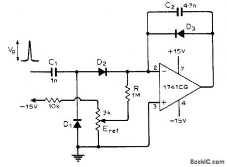
Simple opamp cir-cuit produces time interval proportional to height of positive input pulse, Opamp is con-nected as integrator whose output is held at about zero by negative feedback through D3. Positive input pulse charges C1 and C2, amplifier output steps down, and D3 is reverse-biased. Time for output to charge back up to zero, as observed on oscilloscope, is then directly proportional to input pulse height. Article gives de-sign equations.-G. B. Clayton, Experiments with Operational Amplifiers, Wireless World, Sept. 1973, p 447-448. (View)
View full Circuit Diagram | Comments | Reading(603)
4_BIT_BINARY_TO_5_BIT_BCD
Published:2009/7/7 4:23:00 Author:May
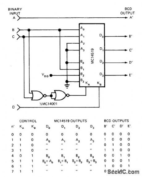
Converts binary number within maohine to BCD value from 0 to 15, for driving visual displays. Requires only quad two-channel data selector with EXCLU-SIVE-NOR function, available in IC packages. Artide gives truth tables and traces operationstep by step.-J. Barnes and J. Tonn, Binaly-to-BCD Converter Implements Simple Algorithm,EDNMagazine, Jan. 5, 1975, p 56, 57, and 59. (View)
View full Circuit Diagram | Comments | Reading(2474)
TELEFAX_PHASING
Published:2009/7/7 4:17:00 Author:May
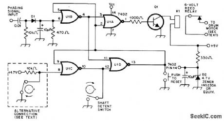
Simple coincidence circuit provides reliable synchronization of Telefax machine in which 2500-Hz signal is generated by photoelectric scanning of paper placed on revolving drum. Circuit uses 7402 quad twoinput NOR gate. If alternate connection enclosed in dashed line is not used, connect pin 8 to ground at pin 7. Q1 is S0014 silicon or equivalent. If relay contacts will handle motor voltage and current, they can be connected directly across points of test switch on machine, with switch left open for phasing circuit to work.-W. C. Smith, A Logic Circuit for Phasing the Telefax, QST, Nov. 1978, p 33-34. (View)
View full Circuit Diagram | Comments | Reading(1434)
TTL_COMPATIBLE_SCHMITT_TRIGGER
Published:2009/7/7 4:15:00 Author:May
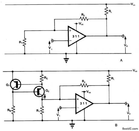

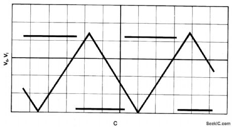


The comparator has an output pull-up resistor RL. and is connected up to operate as a Schmitt trigger using the single rail supply Vcc. The feedback resistors R1 and R2 give upper and lower threshold levels VT+ , VVVTW, respectively. VT+ , is easily set by suitable resistor selection but there is little independent choice of VT- because VT- cannot exceed VCE(SAT) In Fig. 15-13B current-source, comprising the transistors RE, Rg produces a current I~:(VEB/RE), VEB (~0.65 V) being the emitter-base voltage of Q1 and Q2. Fig. 15-13C shows the results of a practical test using the circuit of Fig.15-13B, and the following operating and component data: Vcc=5 V; RL = 1 K ohm; R1=R2=10 K ohm; RB=3.6 K ohm; RE=1K ohm + 10 K ohm pot; Q1=ZTX500; Q2 - ZTX500. (View)
View full Circuit Diagram | Comments | Reading(784)
PUT_LONG_DURATION_TIMER
Published:2009/7/7 4:08:00 Author:May
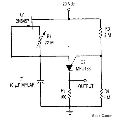
The time circuit can provide a time delay of up to 20 minutes. The circuit is a standard relaxation oscillator with a FET current source in which resistor R1 is used to provide reverse bias on the gate-to-source of the JFET. This tums the JFET off and increases the charging time of C1. C1 should be a low leakage capacitor such as a mylar type.
(View)
View full Circuit Diagram | Comments | Reading(820)
_TIMER_CIRCUIT
Published:2009/7/7 4:08:00 Author:May
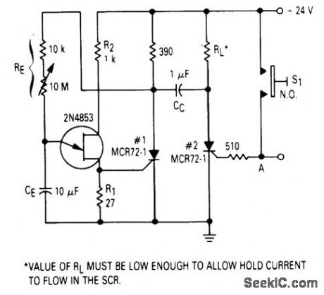
After one cycle of operation, SCR 1 will be on, and a low value of voltage is applied to the UJT emitter circuit, interrupting the timing function. When pushbutton S1 is pushed, or a positive going pulse is applied at point A, SCR 2 will turn on, and SCR 1 will be turned off by commutating capacitor CC. With SCR 1 off, the supply voltage will be applied to RE and the circuit will begin timing again. After a period of time determined by the setting of RE, the UJT witt fire and turn SCR 1 on and commutate SCR 2 off. The time delay is determined by the charge time of the capacitor
(View)
View full Circuit Diagram | Comments | Reading(779)
SERIES_WOUND_MOTOR
Published:2009/7/7 4:06:00 Author:May
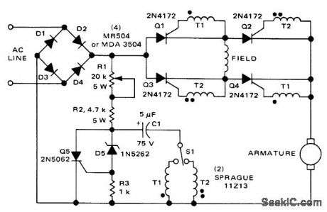
Provides both direction and speed control for fractional-horsepower series-wound or universal DC motors as long as motor current requirements are within SCR ratings. Q1-Q4, connected in bridge, are triggered in diagonal pairs. S1 determines which pair is turned on, to provide direction control. Pulse circuit is used to drive SCRs through T1 or T2. When C1 charges to break-down voltage of zener Q5, zener passes current to gate of SCR Q5 and turns it on. This discharges C1 through T1 or T2 to create desired triggering pulse. Q5 stays on for duration of half-cycle. R1 controls motor speed by changing time required to charge C1, thereby changing conduction angle of Q1-Q4 or Q2-Q3.- Direction and Speed Control for Series, Universal and Shunt Motors, Motorola, Phoenix, AZ, 1976, AN-443. (View)
View full Circuit Diagram | Comments | Reading(2477)
2_hp_THREE_PHASEINDUCTION
Published:2009/7/7 3:59:00 Author:May
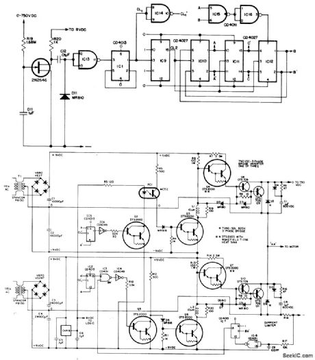
Speed is controlled by applying continuously variable DC voltage to VCO of control circuit for 750-VDC 7-A bridge inverter driving three sets of six Delco DTS-709 duolithic Darlingtons. Bridge inverter circuit for other two phases is identical to that shown for phase AA. VCO output is converted to three-phase frequency varying from 5 Hz at 50 VDC to 60 Hz at 600 VDC for driving output Darlingtons. Optoisolators are used for base drive of three switching elements connected to high-voltage side of inverter.- A 7A, 750 VDC Inverter for a 2 hp, 3 Phase, 480 VAC Induction Motor, Delco, Kokomo, IN, 1977, Application Note 60. (View)
View full Circuit Diagram | Comments | Reading(1586)
LONG_DELAY_LINE_FOR_LOGIC_SIGNALS
Published:2009/7/7 3:55:00 Author:May
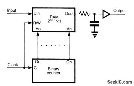

An extremely long delay of logic signal can be accomplished with this circuit. The logic signals to be delayed are applied to the,DIN of RAM. Address lines Ao,A1, . An are connected to outputs Qo, Q1, …… Qn of a binary counter. Clock input of counter and R/W input of RAM are joined together. However, it is sometimes necessary to put an inverter between those inputs, depending on the RAM and counter employed in line. In the first half of clock interval, content on outputs of counter is increased for 1 and content of chosen memory cell is read; in the second half of the clock interval, new content from DIN in the same memory cell is written. When full cycles of counting reaches the same memory cell, again we can read, in the first half of the clock interval of the following counting cycles, the chosen content. Delay time is:
Td=2 n+1·tcl
If clock frequency is not a multiple of input signal frequency, distortion of input signal is proportioned to the clock period. But if the clock frequency is a multiple of input signal frequency, there is no distortion. If we use RAM organized according to 2n+1 x 4 with separated data inputs and data outputs, we can have four parallel long delay lines. The resistor, capacitor, and buffer on DOUT of RAM are used to save output signal in writing time, when output of RAM becomes high impedance. (View)
View full Circuit Diagram | Comments | Reading(795)
FREQUENCY_CONTROLS_SPEED
Published:2009/7/7 3:53:00 Author:May
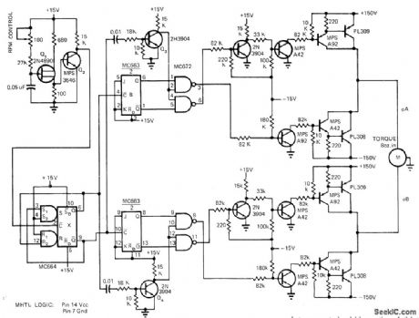
Circuit generates variable frequency between 10 and 300 Hz at constant voltage for changing speed of induction motor between theoretical limits of 300and 9000 rpm without affecting maximum torque. Direct coupling between control and drive circuits is used; if motor noise affects control logic circuits, ptoisolators should be usedbetween control and drive sections. Article tells how circuit works and gives similar circuit using optical coupling.-T. Mazur, Unique Semiconductor Mix Controls Induction Motor Speed, EDN Magazine, Nov. 1, 1972, p 28-31. (View)
View full Circuit Diagram | Comments | Reading(1992)
SPEED_CONTROL_FOR_INDUCTION_MOTOR
Published:2009/7/7 3:40:00 Author:May
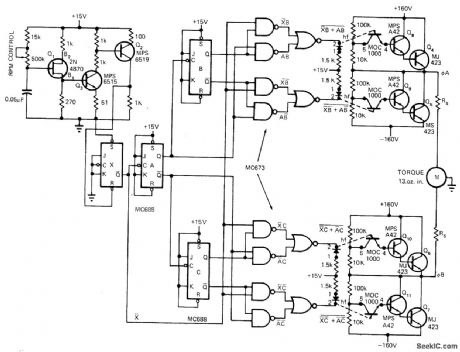
Uses UJT oscillator Q1 to generate frequency in range from 40 to 1200 Hz for feeding to divide-by-4 configuration that gives motor source frequency range of 10 to 300 Hz. With induction motor having two pairs of poles, this gives theoretical speed range of 300 to 9000 rpm with essentially constant torque. Speed varies linearly with frequency. Circuit uses pair of flip-flops (MC673) operated in time-quadrature to perform same function as phase-shifting capacitor so motor receives two drive signals 90° apart. Article covers operation of circuit in detail. Optoisolators are used to provide bipolar drive signals from unipolar control signals. Each output drive circuit is normally off and is turned on only when its LED is on. If logic power fails, drives are disabled and motor is turned off as fail-safe feature.-T. Mazur, Unique Semiconductor Mix Controls Induction Motor Speed, EDN Magazine, Nov. 1, 1972, p28-31. (View)
View full Circuit Diagram | Comments | Reading(998)
SSB_AVERAGE_CURRENT_METER
Published:2009/7/21 21:08:00 Author:Jessie
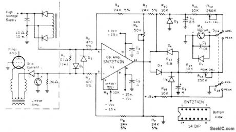
Uses con-trolled time constant of 1/4 s to generate good approximation of average current in voice-modulated SSB signal. Circuit also gives peak current reading, with peaks measured and held for short time. Opamp isolates current from plate supply and converts it into signal that can be run through shaping network to get averages and peaks. D1-D7 are 1N3064 or equivalent. D1 and D2 eliminate spikes that might damage opamp R6 allows small adjustments of opamp gain, which is normally set at 100.-R Sans, Make Your Meter Readings Count,CQ.Dec.1972,P28-29. (View)
View full Circuit Diagram | Comments | Reading(885)
| Pages:246/471 At 20241242243244245246247248249250251252253254255256257258259260Under 20 |
Circuit Categories
power supply circuit
Amplifier Circuit
Basic Circuit
LED and Light Circuit
Sensor Circuit
Signal Processing
Electrical Equipment Circuit
Control Circuit
Remote Control Circuit
A/D-D/A Converter Circuit
Audio Circuit
Measuring and Test Circuit
Communication Circuit
Computer-Related Circuit
555 Circuit
Automotive Circuit
Repairing Circuit