
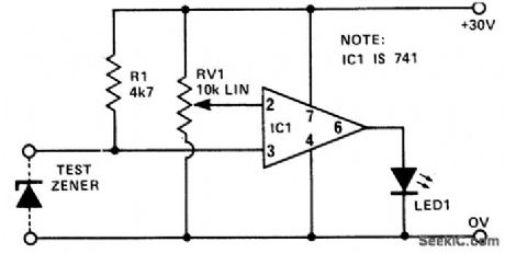
Basic Circuit
Index 330
VHF_MODULATOR
Published:2009/6/25 22:17:00 Author:May
View full Circuit Diagram | Comments | Reading(0)
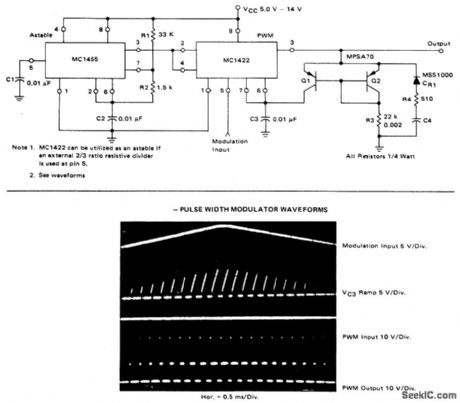
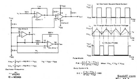
4PULSE_WIDTH_MODULATOR
Published:2009/6/25 22:16:00 Author:May
View full Circuit Diagram | Comments | Reading(729)
3PULSE_WIDTH_MODULATOR
Published:2009/6/25 22:14:00 Author:May
View full Circuit Diagram | Comments | Reading(647)
TONE_DIAL_SEQUENCE_DECODER
Published:2009/6/25 22:14:00 Author:May
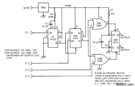
The circuit takes active low inputs from a Touch Tone decoder and reacts to a proper sequence of digits. The proper sequence is determined by which Touch Tone digits the user connects to the sequence decoder inputs TT1, TT2, TT3, and TT4. (View)
View full Circuit Diagram | Comments | Reading(1016)
TONE_DIAL_ENCODER
Published:2009/6/25 22:13:00 Author:May
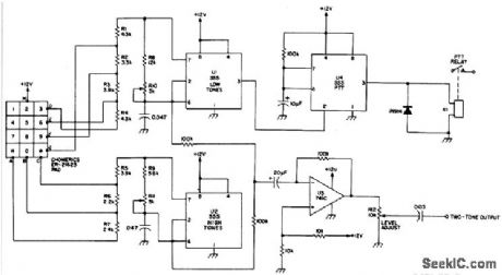
Tone dial encoder with automatic PTT control uses the 555 timers. (View)
View full Circuit Diagram | Comments | Reading(826)
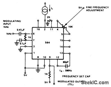
AM_MODULATOR
Published:2009/6/25 22:11:00 Author:May
View full Circuit Diagram | Comments | Reading(870)
2PULSE_WIDTH_MODULATOR
Published:2009/6/25 22:10:00 Author:May
The monostable circuit is triggered by a continuous input pulse train and the threshold voltage is modulated by a control signal. The resultant effect is a modulation of the output pulse width, as shown. A sine-wave modulation signal is illustrated, but any wave-shape could be used. (View)
View full Circuit Diagram | Comments | Reading(910)
MODULATOR_
Published:2009/6/25 22:09:00 Author:May
View full Circuit Diagram | Comments | Reading(746)
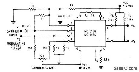
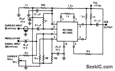
BALANCED_MODULATOR_(+12_Vdc_SINGLE_SUPPLY)
Published:2009/6/25 22:09:00 Author:May
View full Circuit Diagram | Comments | Reading(622)
VIDEO_MODULATOR_
Published:2009/6/25 22:07:00 Author:May

View full Circuit Diagram | Comments | Reading(1582)
LINEAR_PULSE_WIDTH_MODULATOR
Published:2009/6/25 22:07:00 Author:May
View full Circuit Diagram | Comments | Reading(780)
RE_MODULATOR
Published:2009/6/25 22:05:00 Author:May
Capacitors C1, C3, C5, and C6 should be dipped mica. C4 and C7 are compression or piston trimmer types. R6 is PC-board mount trimpot. L1 is 6 tums of No.14 enameled wire, 3/8 inch I.D. by 3/4 inch long, tapped at 1 turn from top. (View)
View full Circuit Diagram | Comments | Reading(779)
HIGH_IMPEDANCE_VlDEO
Published:2009/6/25 22:04:00 Author:May
Compound seriesfeedback circuit using FET at input provides high input impedance and stable wideband gain for general-purpose video amplifier applica-tions.- FET Databook, National Semicon-ductor, Santa Clara, CA 1971, p 6-26-6-36. (View)
View full Circuit Diagram | Comments | Reading(810)
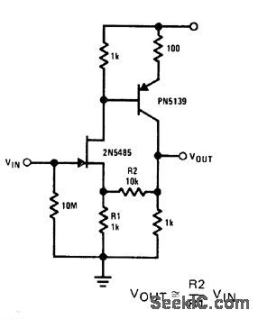
STABILIZED_BIAS
Published:2009/6/25 22:03:00 Author:May
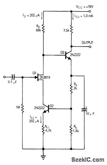
Simple voltage-feedback loop stabilizes bias on direct-coupled FET and bipolar transistor stages. Arrangement uses constant-current source a2 to maintain stable bias voltage on base of 03. By choosing proper resistor values, DC voltage feedback from emitter of bipolar is made to control constant-cur-rent value. Any change in drain current pro-duces opposite change in constant-current value, for stabilizing bipolar. Article gives de-sign equation.-H. T. Russell, DC Feedback Stabilizes Bias on FETTBipolar Pair, EDN Magazine, Nov.15,1970, p 51. (View)
View full Circuit Diagram | Comments | Reading(1166)
1PULSE_WIDTH_MODULATOR
Published:2009/6/25 22:02:00 Author:May
View full Circuit Diagram | Comments | Reading(750)
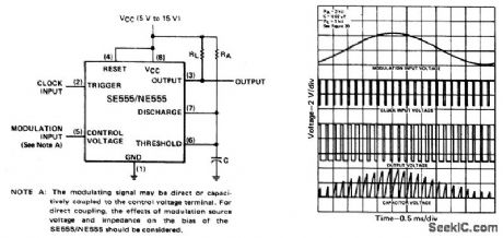
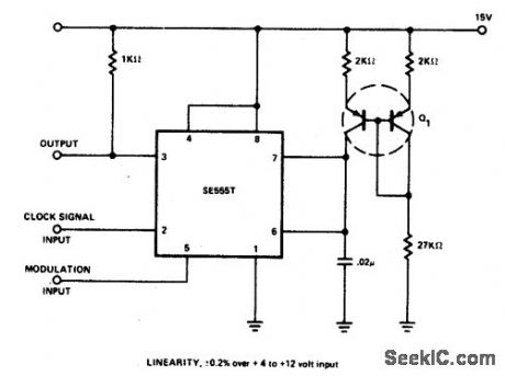
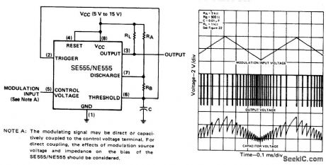
PULSE_WIDTH_MODULATOR
Published:2009/6/25 22:00:00 Author:May
If the timer is triggered with a continuous pulse train in the monostabie mode of operation, the charge time of the capacitor can be varied by changing the control voltage at pin 3.In this manner, the output pulse width can be modulated by applying a modulating signal that controls the threshold voltage. (View)
View full Circuit Diagram | Comments | Reading(0)
TELEPHONE_STATUS_MONITOR_USING_AN_oPTOISOLATOR
Published:2009/6/25 22:00:00 Author:May
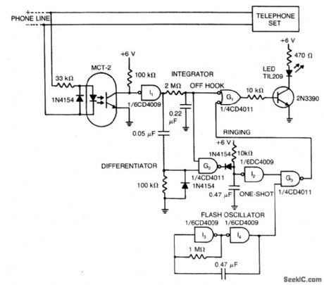
The LED indicates the status of a remote telephone. The light is off if the phone is hung up. It shines steadily if the phone is off hook, and it flashes on and off while phone rings and for 5 seconds after ringing stops. The flashing oscillator operates continuously but can drive the LED only when a ringing signal discharges the one shot capacitor to enable NAND gate G3. Thus, one oscillator handles several phone lines. (View)
View full Circuit Diagram | Comments | Reading(844)
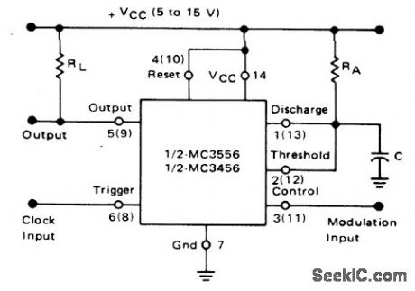
PULSE_POSITION_MODULATOR
Published:2009/6/25 21:58:00 Author:May
The threshold voltage, and thereby the time delay, of a free-running oscillator is shown modulated with a triangular-wave modulation signal; however, any modulating wave-shape could be used. (View)
View full Circuit Diagram | Comments | Reading(2)
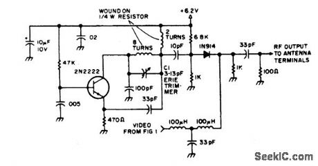
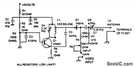
1TV_MODULATOR
Published:2009/6/25 21:56:00 Author:May
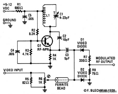
The VHF frequency is generated by a tuned Hartley oscillator circuit. Resistors R2, R3, and R4 bias the transistor, with tapped inductor L1 and trimmercapacitor C1 forming the tank circuit. Adjusting C1 determines the frequdncy. Capacitor C2 provides positive feedback from the tank circuit to the emitter at Q1. Capacitor C4 provides an RF ground for the base of Q1. Bypass capacitor C5 and resistor R1 filter out the radio frequencies generated in the tank circuit to prevent radiation from the power-supply lines. The video signal enters the parallel combination of resistors R5 and R6; this combination closely matches the 75 ohm impedance of most video cables. Resistor R6 is a small screwdrtver-adjusted potentiometer that is used to control the video input level to mixer diodes D1 and D2. (View)
View full Circuit Diagram | Comments | Reading(1315)
HIGH_TOGGLE_RATE_HIGH_FREQUENCY_ANALOG_SWITCH
Published:2009/6/25 21:49:00 Author:May
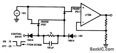
Commutator circuit provides low tmpedance gate drive to the PN4091 analog switch for both on and offdrive conditions.This circuit also approaches the ideal gate drive conditions for high frequency signal handling by providing a low ac impedance for off drive and high ac impedance for on drive to the PN4091 (View)
View full Circuit Diagram | Comments | Reading(0)
| Pages:330/471 At 20321322323324325326327328329330331332333334335336337338339340Under 20 |
Circuit Categories
power supply circuit
Amplifier Circuit
Basic Circuit
LED and Light Circuit
Sensor Circuit
Signal Processing
Electrical Equipment Circuit
Control Circuit
Remote Control Circuit
A/D-D/A Converter Circuit
Audio Circuit
Measuring and Test Circuit
Communication Circuit
Computer-Related Circuit
555 Circuit
Automotive Circuit
Repairing Circuit