
Index 171
HEXFET_SWITCH_CIRCUITS
Published:2009/6/24 3:21:00 Author:May
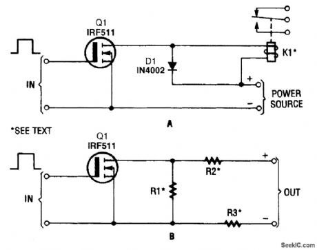
The HEXFET can switch dc power to relays (as shown in A),motors,lamps,and numerous otherdevices That arrangement can even be used to switch resistors in and out ofa circuit,as shown in Fig.88-18B R1,R2,and R3 are possible load resistors and representload configurations that can be used (View)
View full Circuit Diagram | Comments | Reading(891)
SWITCH_DEBOUNCERS
Published:2009/6/24 3:22:00 Author:Jessie
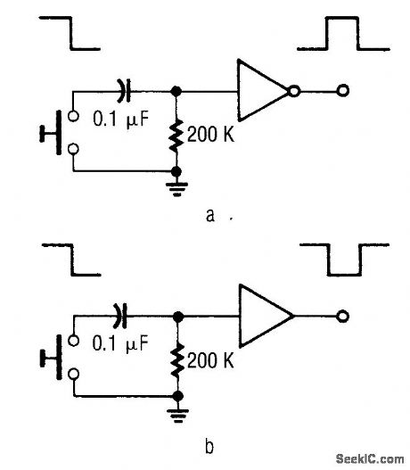
These circuits will cure problems caused by switch-contact bounce. The one shown in Fig.88-21A provides you a positive output pulse, and the one shown in Fig. 88-21B provides you a neg-ative output pulse. (View)
View full Circuit Diagram | Comments | Reading(1363)
AUDIO_CONTROLLED_SWITCH
Published:2009/6/24 3:22:00 Author:Jessie
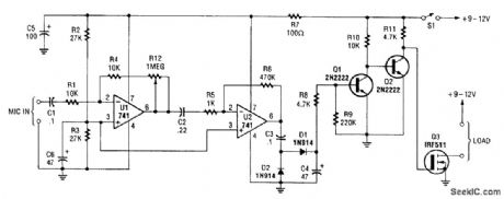
The audio-controlled switch combines a pair of 741 op amps, two 2N222 general-purpose tran-sistors, a HEXFET, and a few support components to produce a circuit that can be used to turn on a tape recorder, a transmitter, or just about anything using sound. (View)
View full Circuit Diagram | Comments | Reading(2590)
AUTO_OFF_POWER_SWITCH
Published:2009/6/24 3:18:00 Author:May
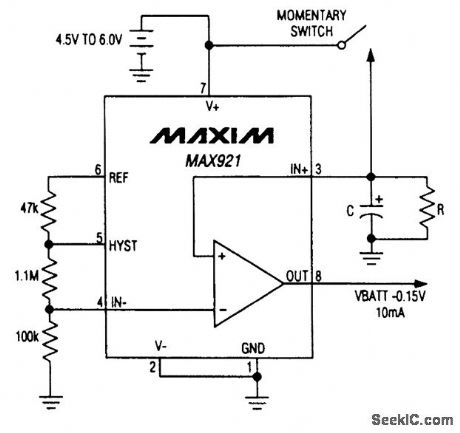
This timed switch circuit can be usedwhere a timed power Source IS needed,The on-time is approximately 4.6RC (View)
View full Circuit Diagram | Comments | Reading(864)
SERIES_SHUNT_PIN_DIODE_RF_SWITCH
Published:2009/6/24 3:17:00 Author:May
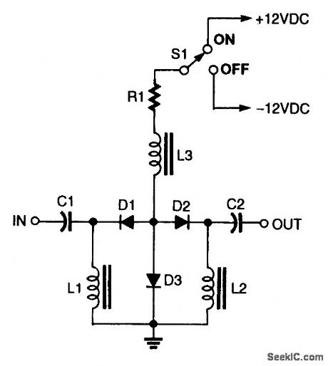
A combination of series and shunt switching, like that shown between the input and output when in the off condition. (View)
View full Circuit Diagram | Comments | Reading(0)
TRANSCEIVER_T_R_SWITCH
Published:2009/6/24 3:17:00 Author:May
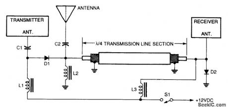
This transceiver's transmit/receive switch uses PIN-diode instead of a relay. On receive, D1 is cut off, D2 is cut off and the antenna connects to the receiver. During transmit, D1 is forward-biased, as is D2. This connects the receiver input. This causes the input impedance of the transmission line to be high, so little transmitter power reaches the receiver. Although not shown in the schematic, the 12-V supply should have a series resistor of 100Ω to 2.2kΩ, depending on diode current, to limit diode current to a safe value. (View)
View full Circuit Diagram | Comments | Reading(0)
PIN_DIODE_SWITCH
Published:2009/6/24 3:16:00 Author:May
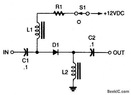
This PIN diode switch uses RF chokes and a single diode。R1 is typically 470Ω to 2.2kΩ (View)
View full Circuit Diagram | Comments | Reading(0)
RESISTOR_PIN_DIODE_SWITCH
Published:2009/6/24 3:13:00 Author:May
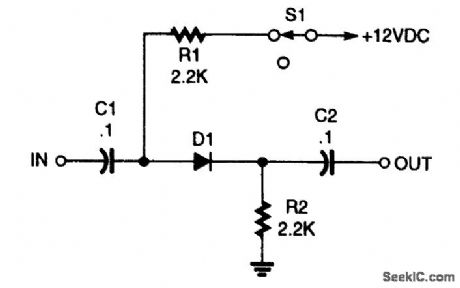
This circuit uses resistors instead of RE chokes to keep costs low. The values of R1 and R2 should be no lower than about 1 kΩ to minimize loss. (View)
View full Circuit Diagram | Comments | Reading(0)
FULL_WAVE_SPEED_CONTROL_FOR_MOTORS
Published:2009/6/24 3:13:00 Author:May
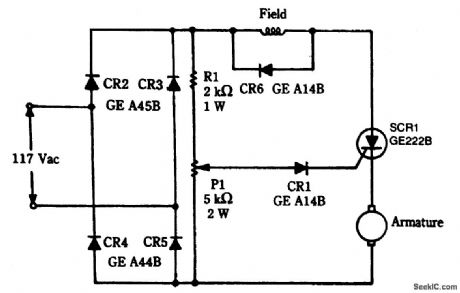
A bridge rectifier provides pulsating dc to a universal motor, and the SCR is used as a phase-con-trolled switch. This circuit allows smoother operation of the motor at low speeds. (View)
View full Circuit Diagram | Comments | Reading(1770)
RECEIVER_BANDSWITCHING
Published:2009/6/24 3:13:00 Author:May
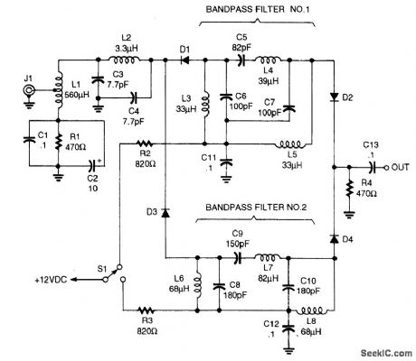
Eight-band receiver front-end selection can be accomplished by using PIN diode switches (View)
View full Circuit Diagram | Comments | Reading(737)
SHUNT_PIN_DIODE_SWITCH
Published:2009/6/24 3:12:00 Author:May
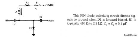
This PlN-diode switching circuit directs sig-nals to ground when D1 is forward-biased. R1 is Lypically 470Ω to 2.2kΩ. C1 = C2 =0.1μF. (View)
View full Circuit Diagram | Comments | Reading(892)
ANALOG_SWITCH
Published:2009/6/24 3:11:00 Author:May
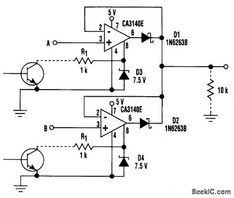
This design takes advantage of the strobed output stage of a CA3140 amplifier. With the strobing capability, the circuit's output voltage can be set to either of the input voltages by grounding one of the control inputs, either A or B.When the strobe input at pin 8 is taken below 1V, that amplifier is disabled. The remaining am-plifier then acts as a unity-gain high-impedance buffer.The 10-kΩ output resistor enables the output voltage to swing down to 20 mV from ground. The Zener-diode clamps and associated resistors connected at the strobe inputs can be omitted for the lowest-cost applications. However, experience has shown that they allow the amplifiers to shrug off the effect of high transient voltages.The circuit is particularly suited to 8-bit microcontroller applications, where the strobe inputs can be driven directly from two open-collector output ports under software control.The use of Schottky diodes for Dl and D2 makes possible an output swing of 2.5 V when the circuit is powered from a 5-V supply. (View)
View full Circuit Diagram | Comments | Reading(2028)
SERIES_SHUNT_PIN_DIODE_RF_SWITCH
Published:2009/6/24 3:17:00 Author:Jessie
A combination of series and shunt switching, like that shown between the input and output when in the off condition. (View)
View full Circuit Diagram | Comments | Reading(2264)
TRANSCEIVER_T_R_SWITCH
Published:2009/6/24 3:17:00 Author:Jessie
This transceiver's transmit/receive switch uses PIN-diode instead of a relay. On receive, D1 is cut off, D2 is cut off and the antenna connects to the receiver. During transmit, D1 is forward-biased, as is D2. This connects the receiver input. This causes the input impedance of the transmission line to be high, so little transmitter power reaches the receiver. Although not shown in the schematic, the 12-V supply should have a series resistor of 100Ω to 2.2kΩ, depending on diode current, to limit diode current to a safe value. (View)
View full Circuit Diagram | Comments | Reading(1847)
PIN_DIODE_SWITCH
Published:2009/6/24 3:16:00 Author:Jessie
This PIN diode switch uses RF chokes and a single diode。R1 is typically 470Ω to 2.2kΩ (View)
View full Circuit Diagram | Comments | Reading(1774)
SCR_MOTOR_SPEED_CONTROL
Published:2009/6/24 3:16:00 Author:Jessie
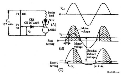
An SCR is used in a phase-control type application to supply a variable pulsating dc voltage to a motor. (View)
View full Circuit Diagram | Comments | Reading(2609)
DIGITALLY_CONTROLLED_ONE_OF_FOUR_ANALOG_SWITCH
Published:2009/6/24 3:15:00 Author:Jessie
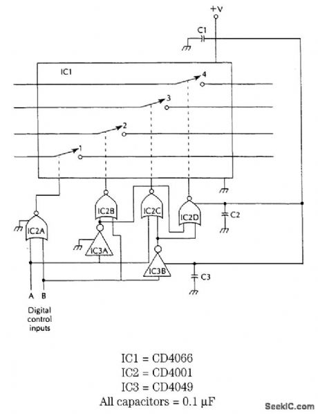
View full Circuit Diagram | Comments | Reading(1208)
BASIC_ZERO_CROSSING_SWITCH_CIRCUIT
Published:2009/6/24 3:10:00 Author:May
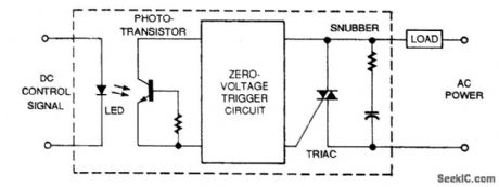
Here is the schematic of a solid-state ac relay with zero-crossing. The triac permits the relay to switch to ac directly. (View)
View full Circuit Diagram | Comments | Reading(0)
INVERTING_POWER_AMPLIFIER
Published:2009/6/24 3:14:00 Author:Jessie
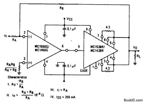
View full Circuit Diagram | Comments | Reading(0)
RESISTOR_PIN_DIODE_SWITCH
Published:2009/6/24 3:13:00 Author:Jessie
This circuit uses resistors instead of RE chokes to keep costs low. The values of R1 and R2 should be no lower than about 1 kΩ to minimize loss. (View)
View full Circuit Diagram | Comments | Reading(1374)
| Pages:171/312 At 20161162163164165166167168169170171172173174175176177178179180Under 20 |
Circuit Categories
power supply circuit
Amplifier Circuit
Basic Circuit
LED and Light Circuit
Sensor Circuit
Signal Processing
Electrical Equipment Circuit
Control Circuit
Remote Control Circuit
A/D-D/A Converter Circuit
Audio Circuit
Measuring and Test Circuit
Communication Circuit
Computer-Related Circuit
555 Circuit
Automotive Circuit
Repairing Circuit