
Index 172
LONG_TIME_DELAY_MOTOR_CONTROL_CIRCUIT
Published:2009/6/24 3:05:00 Author:May
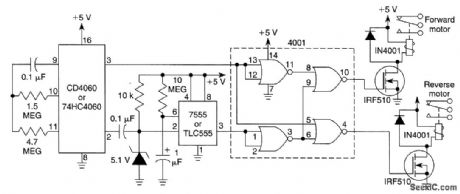
Circuit controls forward and reverse motors.Every hour, one motor runs for 10 seconds. (View)
View full Circuit Diagram | Comments | Reading(1023)
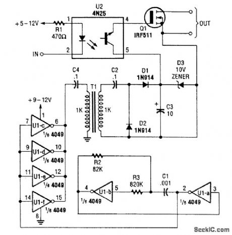
ISOLATED_SWITCH
Published:2009/6/24 3:05:00 Author:May

This dc-controlled switch uses an optoisolator/coupler,U1,to electrically isolate the input signalfrom the output control device. (View)
View full Circuit Diagram | Comments | Reading(1301)
BASIC_ZERO_CROSSING_SWITCH_CIRCUIT
Published:2009/6/24 3:10:00 Author:Jessie
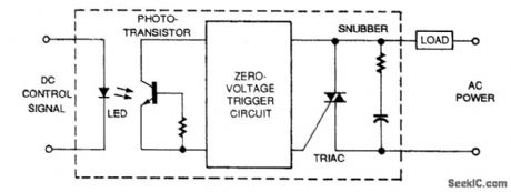
Here is the schematic of a solid-state ac relay with zero-crossing. The triac permits the relay to switch to ac directly. (View)
View full Circuit Diagram | Comments | Reading(2981)
OSCILLATOR_TRIGGERED_SWITCH
Published:2009/6/24 3:09:00 Author:Jessie
In this circuit (the oscillator-triggered switch), the generated by an astable oscillator. (View)
View full Circuit Diagram | Comments | Reading(2585)
OP_AMP_AND_ANALOG_SWITCH_RON_COMPENSATOR
Published:2009/6/24 3:08:00 Author:Jessie
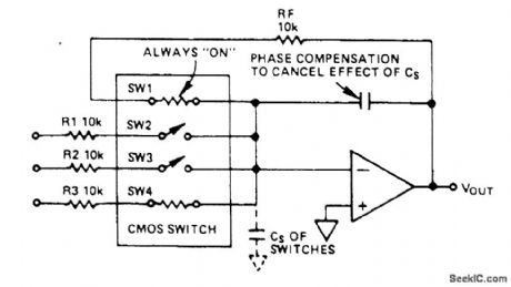
This switch is in series with feedback resistor to compensate gain. (View)
View full Circuit Diagram | Comments | Reading(0)
LOW_OUTPUT_IMPEDANCE_MULTIPLEXER
Published:2009/6/24 3:08:00 Author:Jessie
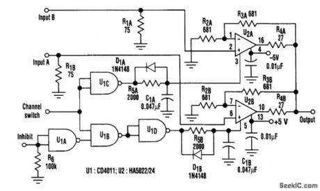
Both inputs are terminated in their characteristic impedance; 75Ω is typical for video applications. Because the output cables usually are terminated in their characteristic impedance, the gain is 0.5. Consequently, amplifiers U2A and U2B are configured in a gain of +2 to set the circuit gain at 1.R2 and R3 determine the amplifier gain; if a different gain is desired, R2 should be changed according to the equation G = (1 + R3/R2) R5, LCL1, and D1 make up an asymmetrical charge/discharge time circuit that configures U1 as a break-before-make switch to prevent both amplifiers from being ac-tive simultaneously. The multiplexer transition time is approximately 15μs with the component values shown. (View)
View full Circuit Diagram | Comments | Reading(1547)
STEPPER_MOTOR_PULSE_GENERATOR
Published:2009/6/24 2:59:00 Author:Jessie
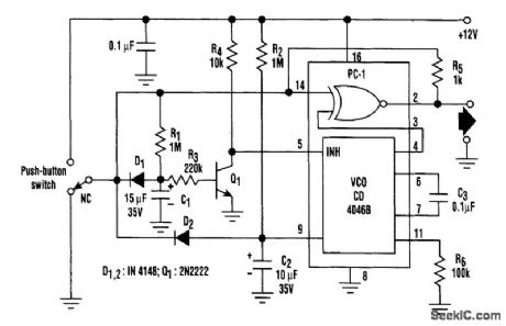
When the switch is in its normally closed (NC) position, capacitors C1 and C2 are held discharged by diodes Dl and D2. Switching off transistor Q1 inhibits the voltage-controlled oscillator of the PLL. The two inputs and, hence, the output of the EX-OR gate (phase comparator 1) ofthe PLL remain at the logic 0 level.When the pushbutton is pressed, C1 and C2 are allowed to charge via resistors R1 and R2. The VCO is enabled only after a time delay (≈0.5 second) set by R1, R3, and C1. During this delay period, the EX-OR gate output follows the logic level at the switch output. As a result, one-shot pulses can be generated by pressing the pushbutton, then releasing it within 0.5 second. R5 provides the switch-debouncing function.If the pushbutton is pressed for more than 0.5 second, the VCO is enabled. The rising voltage at the control input (pin 9) causes a linear increase in VCO frequency and thus accelerates the step-per motor. Releasing the pushbutton discharges C1 and C2 and inhibits the VCO. (View)
View full Circuit Diagram | Comments | Reading(0)
ACCURATE_MOTOR_SPEED_CONTROL
Published:2009/6/24 2:57:00 Author:Jessie
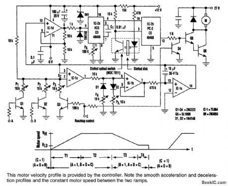
This circuit can control dc motors used in machines that pull materials, such as wire, yam, film, etc., from the supply rolls and rewind them onto smaller rolls. Its motor velocity profile is shown in the figure.A lightweight disk with at least 32 slots is mounted on the motor shaft. It works in a slotted op-tical switch (MOC7811) to sense the motor speed. Phase comparator 2(PC-2)of the phase-locked loop(IC-CD 4046B)compares the frequency (fV)at the output of the VCO with the pulse rate (fm) at the optical switch output. The PC-2 output drives the motor via the transistors when fm>fv, and removes the supply to the motor when fv>fm. The drive system quickly reaches an equilibrium con-dition when fm=fv.Op amps IC-1a, 1b, and 1c form a tracking integrator whose output always smoothly reaches and remains at a voltage equal to the command voltage (Ec) presented at the inverting input of op-amp IC-1a. When the digital control inputs are set to (A=1,B=0=C), the integrator generates a posi-tive slope ramp that sweeps the VCO frequency and, thus, accelerates the motor. The acceleration rate and the constant speed VHI, can be adjusted by presets P4 and PI, respectively.Similarly, when the inputs are set to (A=0=C,B=1), the integrator generates a negative slope ramp that decelerates the motor. Presets P5 and P2 can be adjusted to set the required deceleration and the constant speed VLO, respectively. (View)
View full Circuit Diagram | Comments | Reading(3048)
SHARP_SQUARE_WAVEFORMS_FROM_MULTIVIBRATOR
Published:2009/6/24 2:50:00 Author:Jessie
By using diodes as shown, the loading effect on the collector of the transistors caused by the tim-irtg capacitors can be avoided. As the collector of the transistors rises toward VCC the diode discon-nects the tinting capacitors. (View)
View full Circuit Diagram | Comments | Reading(1287)
SQUARE_WAVE_GENERATOR
Published:2009/6/24 2:50:00 Author:Jessie
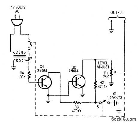
A 60-Hz waveform from T1 drives an audio amplifier to clipping. Output is 60 Hz with about 0- to 1.4-V p-p amplitude. (View)
View full Circuit Diagram | Comments | Reading(0)
SIMPLE_NOISE_LIMITER_FOR_RECEIVERS
Published:2009/6/24 2:48:00 Author:Jessie
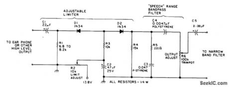
This circuit uses a diode series clipper to limit noise peaks on a received signal. It is best used, where several volts p-p of audio signal are available. (View)
View full Circuit Diagram | Comments | Reading(724)
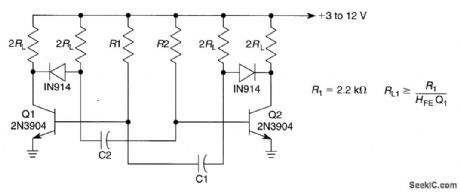
PRECISE_dc_MOTOR_SPEED_CONTROLLER
Published:2009/6/24 2:39:00 Author:May
A series dc motor can be made to have the same characteristics as an ac synchronous motor using this circuit. This control technique is useful where a constant motor speed is needed. (View)
View full Circuit Diagram | Comments | Reading(2535)
Automatic Sprinkling Irrigation Controller (7)
Published:2011/7/14 5:56:00 Author:Sue | Keyword: Automatic, Sprinkling Irrigation, Controller
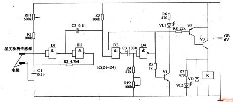
When the soil humidity is proper, the resistance value between the humidity detector's two probes is small. D1's input terminal has low level and the schmitt trigger cannot be triggered. Then D4 outputs high level which will make V1 and V2 disconnected. K is not connected and the water pump doesn't work. VL2 is not illuminated. At the same time, V3 is connected, VL1 is illuminated which indicates that the soil humidity is proper.
When the soil humidity is low enough, and the resistance value between the humidity sensor's two probes reaches a certain given value, the schmitt trigger will be reversed. The monostable trigger will get a negative skipping pulse through C2 which will make the monostable trigger reversed. D4 will output low level which will make V3 disconnected. VL1 is illuminated. V1 and V2 are connected and K is connected. The water pump begins to work. At the same time VL2 will be illuminated indicating that it is sprinkling. (View)
View full Circuit Diagram | Comments | Reading(733)
Automatic Sprinkling Irrigation Controller (5)
Published:2011/7/14 5:53:00 Author:Sue | Keyword: Automatic, Sprinkling Irrigation, Controller
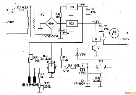
The 220v ac voltage will generate +12v voltage and +9v voltage after it is reduced by T,rectified by VD1-VD4, stablized by IC1,IC2. The voltages will be provided to the relay K and IC3 respectively.
When to detect soil's humidity, we should stick the humidity detector's two probes into the detected soil(the distance between the two probes are 1-2mm). When the humidity is high, and it reaches the given standard, the resistance value between the humidity detector's two probes is becoming smaller which will make NOT GATE D1's input terminal have high level while the output terminal will have low level. V is disconnected. The relay K doesn't work. The electric motor M doesn't work.
When the soil humidity is becoming low, the resistance value between the humidity detector's two probes is becoming higher which will make NOT GATE D1's input terminal have low level while the output terminal will have high level which will make V connected. K is connected. The electric motor begins to work and the equipment of sprinkler irrigation will begin to work. (View)
View full Circuit Diagram | Comments | Reading(723)
Multi Control Switch Circuit Composed of CD4017
Published:2011/7/27 5:37:00 Author:Sue | Keyword: Multi Control, Switch
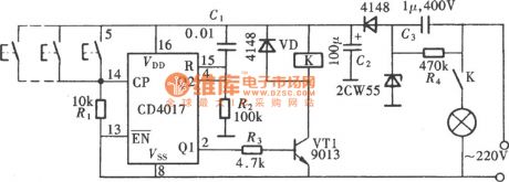
The picture shows the multi control single bond control switch circuit. Usually, we always use bistable flip-flop to compose a switch control circuit which can be on as well as be off. (View)
View full Circuit Diagram | Comments | Reading(855)
Jitter Buffer Switch Circuit Composed of CD4013
Published:2011/7/27 5:38:00 Author:Sue | Keyword: Jitter Buffer, Switch
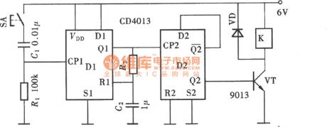
The picture shows the jitter buffer switch circuit composed of CD4013. It uses half of dual D flip-flop to compose bistable control circuit, uses the other half of theflip-flop to compose monostable time delay circuit, and uses one CD4013 to compose a control circuit with complete function. (View)
View full Circuit Diagram | Comments | Reading(4899)
Sound Controlled Time Delay Energy Saving Switch Circuit Composed of CD4069
Published:2011/7/27 5:38:00 Author:Sue | Keyword: Sound Controlled, Time Delay, Energy Saving
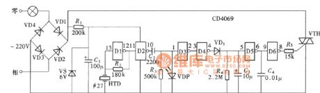
This sound controlled switch has high trigger sensitivity, and it can be triggered by people's footstep and it will close automatically after time delay of 20s. It works well, convenient and energy saving. The circuitconsists ofone hex inverter CD4069, piezoelectric acoustic sensor and one bidirectional thyristor with simple structure. It is economic and convenient with great promotion value. The picture shows the circuit which consists of acoustic sensor, voltage amplifier, light control circuit, delay circuit, thyristor and its trigger circuit. (View)
View full Circuit Diagram | Comments | Reading(1060)
Division Circuit 4(XR-2228)
Published:2011/7/27 5:38:00 Author:Sue | Keyword: Division Circuit
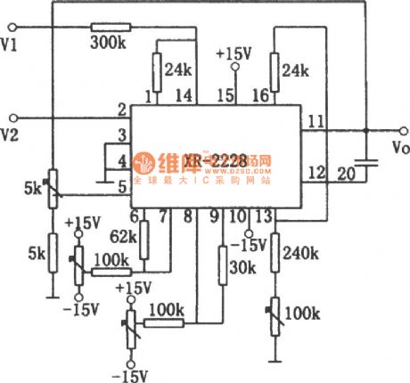
As seen in the figure, the division circuit consists of monolithic multiplier integrated circuit XR-2228. The relation between the output signal V1 and input signal V2 is: Vo=10V1/V2.
The input signal V1 can be either positive or negative but V2 must be negative. If V2 is positive, the circuit will be locked (but it will not broke the integrated package). Every potentiometer is used to adjust the circuit so that it can work at the best working state. At the same time, it can use the known reference voltage to check the circuit. (View)
View full Circuit Diagram | Comments | Reading(735)
Division Circuit Composed of NE555
Published:2011/7/27 5:38:00 Author:Sue | Keyword: Division Circuit
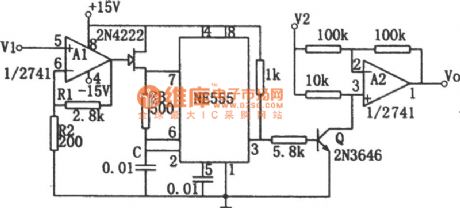
The picture shows the division circuit composed of voltage-frequency converter and amplitude modulator. The input voltage V1 controls field effect tube 2N4222's inner resistance value through operational amplifier A1, so the oscillate frequency of the nonstable multivibrator will be changed.A2 is the amplitude modulator. After the input signal V2 is modulated, it will be output. Presume field effect tube's pinch-off voltage is Vp. If Vp=(1+R1/R2), then the relation between input and output is : Vo=-V2/V1. V1 and V2 are required to have a range of 0-10V. The output Vo is an average value which can be obtained through the filter. It can also be obtained by reading the damped voltmeter. (View)
View full Circuit Diagram | Comments | Reading(647)
Sub-ultrasonic Remote Control Switch(NE555,LM567,CD4013) Circuit
Published:2011/7/29 5:47:00 Author:Sue | Keyword: Sub-ultrasonic, Remote Control
Signal with a frequency higher than 20kHz always can't be heard by human ears, so it is called ultrasonic wave. But in fact, signals with a frequency between 18-20kHz is also hard for human ears to recognise, espacially for those with small transmitting power, which is hardly heard by human ears. So signalsin this range is also called sub-ultrasonic signal. By using sub-ultrasonic signal as remote control signal, special ultrasonic receiver and transmitter are not needed, and human hearings will not be disturbed, so it is very economic and convenient. (View)
View full Circuit Diagram | Comments | Reading(2558)
| Pages:172/312 At 20161162163164165166167168169170171172173174175176177178179180Under 20 |
Circuit Categories
power supply circuit
Amplifier Circuit
Basic Circuit
LED and Light Circuit
Sensor Circuit
Signal Processing
Electrical Equipment Circuit
Control Circuit
Remote Control Circuit
A/D-D/A Converter Circuit
Audio Circuit
Measuring and Test Circuit
Communication Circuit
Computer-Related Circuit
555 Circuit
Automotive Circuit
Repairing Circuit