
Index 177
SIMPLE_HF_RECEIVE_CONVERTER
Published:2009/6/22 23:38:00 Author:Jessie
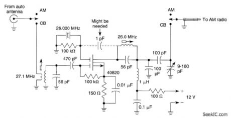
Designed for CB reception, this crystal-controlled converter uses one 40820 dual-gate MOSFET. The circuit will work with any crystal either 3rd overtone or fundamental, over 1 to 50 MHz. (View)
View full Circuit Diagram | Comments | Reading(1953)
SECURITY_ALARM
Published:2009/6/22 23:38:00 Author:Jessie
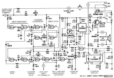
This alarm features open- and closed-loop detector and automatic alarm shutoff. Offers 15 second exit/entrance delay. Alarm on time can be adjusted from 1 to 15 minutes. (View)
View full Circuit Diagram | Comments | Reading(1429)
AUTOMOTIVE_BURGLAR_ALARM
Published:2009/6/22 23:35:00 Author:Jessie
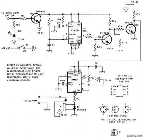
Alarm triggers on after a 13 second delay and stays on for 1-1 1/2 minutes. Then it resets automatically. It can also be turned off and reset by opening and reclosing S1. (View)
View full Circuit Diagram | Comments | Reading(1198)
SIMPLE_EVENT_COUNTER
Published:2009/6/22 23:03:00 Author:May
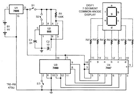
S1 is a power switch. U2 drives counter U3 by producing a pulse when S2 is depressed. U4 and DISP1 read the count of counter IC U3. S3 is a reset to zero switch. The counter is a basic one-digit circuit useful as a holding block or by itself. (View)
View full Circuit Diagram | Comments | Reading(4068)
MICROPROCESSOR_SUPERVISORY_CIRCUIT
Published:2009/6/22 23:03:00 Author:May
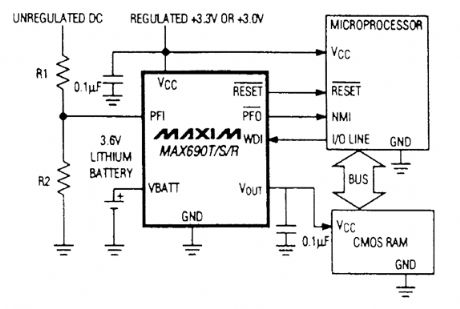
This circuit provides a reset pulse during power up, down, or low-voltage battery back up, switching, a watchdog timer and a 1.25-V threshold detector for power failure or power fail warning, or to monitor another supply. (View)
View full Circuit Diagram | Comments | Reading(0)
COMPUTALARM
Published:2009/6/22 23:25:00 Author:Jessie
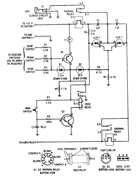
The circuit has a built-in, self-arming feature. The driver turns off the ignition, presses the arm button on the Computalarm, and leaves the car. Within 20 seconds, the alarm arms itself-all automatically! The circuit will then detect the opening of any monitored door, the trunk lid, or the hood on the car. Once acti-vated, the circuit remains dormant for 10 sec-onds. When the 10-second time delay has run out, the circuit will close the car's horn relay and sound the ham in periodic blasts (approxi-mately 1 to 2 seconds apart) for a period of one minute. Then the Computalarm automatically shuts itself off (to save your battery) and re-arms. If a door, the trunk lid, or the hood re-mains ajar, the alarm circuit retriggers and another period of horn blasts occurs. The Com-putalarm has a key switch by which the driver can disarm the alarm circuit within a 10-second period after he enters the door. The key switch consists of a closed circuit jack, J1, and a mating miniature plug. (View)
View full Circuit Diagram | Comments | Reading(1582)
ATMOSPHERE_NOISE_MONITOR
Published:2009/6/22 23:21:00 Author:Jessie
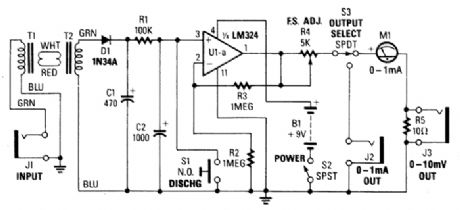
Tune an unmodified transistor radio to an unused frequency near 540 kHz that's free of broad-cast-station interference; the receiver is used to pick up sferics. The received signal is fed from the receiver's earphone jack through a patch cord to the input jack(J1)of the circuit. The back-to-back audio transformers, T1 and T2, provide a suitable impedance match and signal level when the unit is used with various receivers.Diode Dl rectifies the audio input from the receiver to pulsating dc, which is filtered by C1, R1, and C2 to provide a time constant of several minutes. That dampens out fluctuations in most cases, unless lightning flashes are very infrequent.The voltage appearing at the output of the filter is a function of signal strength transferred by C1.Switch 51 is included to prgvide a convenient way to discharge the capacitors, if adjustments are re-quired during a monitoring session.Integrated circuit U1(one section of an LM324 quad pro op amp)is used as a high input-resis-tance voltmeter. Resistors R2 and R3 determine amplifier gain, and potentiometer R4 is used to ad-just full-scale meter deflection for a suitable voltage level at the input. A value of 1.5 V has been satisfactory for use with several receivers tried, but they can be changed.If the monitor is to be used only as a meter, the milliammeter can be connected directly between R4 and chassis ground, omitting R5, 53, J2, and J3. The latter components provide suitable output for use with a chart recorder having a full-scale range of either 10 mV or 1 mA. The circuit, when powered from a 9-V battery, draws about 1 mA. (View)
View full Circuit Diagram | Comments | Reading(1413)
HUM_REDUCER_FOR_DIRECT_CONVERSION_RECEIVERS
Published:2009/6/22 23:20:00 Author:Jessie
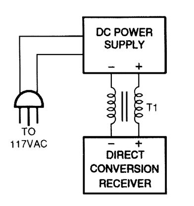

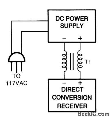
One cure for ac power line hum and ripple (caused by leakage current) is to use a well-regulated and filtered 9- to 18-Vdc power supply with a balancing choke (T1 in this illustration) between the power supply and the DCR. (View)
View full Circuit Diagram | Comments | Reading(1571)
PG_PASSWORD_PROTECTOR
Published:2009/6/22 23:01:00 Author:May
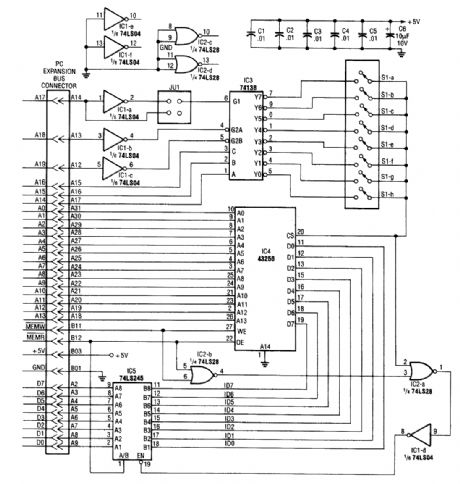
IC4, a static RAM, is mounted in a smart built-in switch over circuitry. This retains SRAM con-tents when power is off. The rest of the circuitry consists of address decoding logic and jumper JU1, used to decode a 16K address space for the 32K static RAM. Software is necessary and this is con-tained in the original article (see reference). (View)
View full Circuit Diagram | Comments | Reading(0)
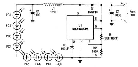
RECHARGEABLE_SOLAR_POWER_FOR_SUN_TRACKER
Published:2009/6/22 23:01:00 Author:Jessie
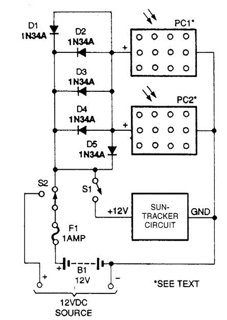
This application circuit provides rechargeable solar power for the sun tracker, as well as for another 12-volt device. PC1 and PC2 can be mounted on sun tracker assembly. (View)
View full Circuit Diagram | Comments | Reading(0)
PHOTODIODE_LOG_CONVERTER_TRA_NSMITTER
Published:2009/6/22 23:00:00 Author:Jessie
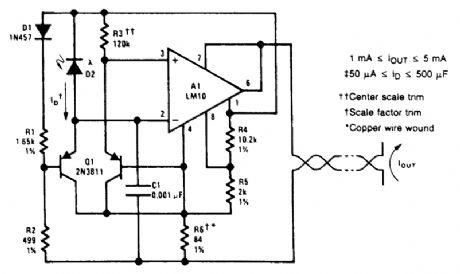
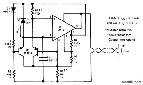
A logarithmic conversion is made on the output current of a photodiode to compress a fourdecade, light-intensity variation into a standard transmission range. The circuit is balanced at midrange, where R3 should be chosen so that the current through it equals the photodiode current. The log-conversion slope is temperature compensated with R6. Setting the reference output to 1.22 V gives a current through R2 that is proportional to absolute temperature because of D1 so that this level-shift voltage matches the temperature coefficient of R6. C1 has been added so that large-area photodiodes with high capacitance do not cause frequency instabilities. (View)
View full Circuit Diagram | Comments | Reading(1372)
SOLAR_POWER_SUPPLY_WITH_LINEAR_REGULATOR
Published:2009/6/22 22:58:00 Author:Jessie
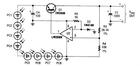
This regulator delivers a constant 2.4 Vdc for powering small devices that run on two AA cells, such as cassettes and small radios. Regulator drop is about 0.3 volt. This should be considered when choosing solar cells. Load current is typically 125 mA. (View)
View full Circuit Diagram | Comments | Reading(0)
The automatic control circuit diagram of vestibular light with photocoupler
Published:2011/3/30 22:53:00 Author:Ecco | Keyword: automatic control, vestibular light , photocoupler

According to the circuitry, A stands for four sets of analog electronic switches(S1~S4: the parallel connection of S1,S2,S3 is used as time-delay circuit, which could increase the driving power and anti-interference capability. When they are connected to the power, and they could control vestibular light H directly by bidirectional triode thyristor VT with driving of R4,B6; S4 and light dependent resistor Rl. etc composed environmental light measuring circuitry. When the door is closed, the reed KD in the door will influenced by magnet, its contacts will be disconnected, and S1, S2, S3 are in the state of ON . When in the night, the host come back and open the door, the magnet will separated from KD, and the contacts will be connected. At the same time, the 9V supply will charge C1 by passing R1, the voltage in two terminals rise to 9V quickly, and commutating voltage passes S1,S2,S3 and R4 to make B6 lighted and bidirectional triode thyristor breakovered. H is lit. That is torealize automatic control. When the door in closed, the magnet will make the contacts of KD disconnected, and 9v supply will stop charging for C1, the circuitry is in the time-delay state. C1 begin discharges to the R3, after a period of time delay, the two terminal voltage of C1 will lower than opening voltage(1.5V) of S1,S2,S3, and they will recover the disconnected state, and B6 and H stop working. That is to realize the function of turning off a lamp while postponing.
(View)
View full Circuit Diagram | Comments | Reading(752)
SET_TIME_WINDOWS_WITHIN_A_CLOCK
Published:2009/6/22 22:49:00 Author:Jessie
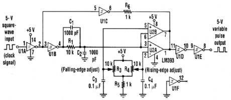
At times, it is necessary to produce pulses of adjustable width and whose start times might vaty with reference to a master clock. The input signal is inverted and buffered by U1A, while U1B and U1C reinvert the signal to produce square, buffered renditions of the input signal. Potentiometers R3 and R4 set references for the comparators.The input polarity of U2A keeps its output transistor tumed on until the voltage at the nonin-verting input exceeds the reference set by R4 (the rising edge adjustment). When this reference voltage is exceeded, the output transistor is turned off and the output signal is pulled up via R6.Meanwhile, the input polarity of U2B keeps its output transistor turned off until the voltage at the in-verting input exceeds the reference set by R3 (the falling edge adjustment). When this reference voltage is surpassed, the output transistor of U2B is turned on, pulling the output signal low through the wired-OR conftguration of U2. The output of U2 is then double-inverted and buffered by U1D and U1E. What results is a pulse whose start time (rising edge) can be adjusted by R4, and whose stop time (falling edge) can be adjusted by R3.The output of the comparators is pulled up to the input waveform through resistor R6 to U1C.This prevents the comparators from switching during the low cycle of the input waveform, regard-less of the positions of R3 and R4. This has the effect of locking out changes during the low period of the input signal, and would probably require additional logic if it were done strictly in the digital domain.The circuit, with the component values shown, works well between about 50 and 150 kHz. (View)
View full Circuit Diagram | Comments | Reading(1316)
LOW_FREQUENCY_CLOCK
Published:2009/6/22 22:50:00 Author:May
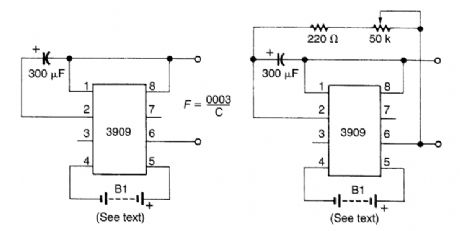
The LM3090 is an LED flasher IC that is designed to oscillate at low frequencies. The clock out-put of the first circuit can be changed by changing the value of the capacitor, and the second circuit lets you adjust the frequency with the trimmer. BI can be one or two alkaline 1.5-V cells. The LM3909 can supply up to 45-mA pulses at greater than 2V. (View)
View full Circuit Diagram | Comments | Reading(952)
ALARM_DIALER
Published:2009/6/22 22:48:00 Author:May
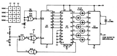
This circuit dials a stored DTMF tone sequence from EPROM when a control line is taken to 0 V. IC1 is a Schmitt trigger oscillator, running at around 2 Hz. It clocks a 4024 binary counter. The coun-ter's outputs connect to the address leads of the EPROM. A 2716 was used here, but the choice of EPROM is by no means critical.Normally, the counter is held reset by a logic 1 on its reset pin (pin 2). When the trigger input is sent low, pin 10 of IC1 goes low, pin 3 goes high, and the reset is removed from the counter. It then begins to clock, incrementing the EPROM. When moved from address 000000, the data on bit DO of the EPROM changes to a logic 1 and holds the circuit running. The last address should have data 11111110 to reset the circuit to standby. (View)
View full Circuit Diagram | Comments | Reading(0)
SELF_RETRIGGERING_TIMED_ON_GENERATOR
Published:2009/6/22 22:47:00 Author:May

When power is first applied to the circuit, CZ begins to charge via LED1, R3, and R4. When the voltage across C2 reaches UI's input trigger level, the output of UI at pin 6 goes positive for a period that is determined by the values of C1 and R1. That turns Q1 on, discharging C2 through Dl and Q1.
At the end of the set period, the output of UI at pin 6 goes low, turning Q1 off and allowing the current to begin flowing through LED1, R3, and R4 to gain charge C2, causing the cycle to repeat.The repeat time is determined by the values of R3, R4, and C2. The previous formula won't be as accurate for this circuit, but it will at least get you close enough for the capacitor value; then R4, can be fine-tuned to obtain the desired timing period. (View)
View full Circuit Diagram | Comments | Reading(0)
PROGRAMMABLE_LIGHT_ACTIVATED_RELAY
Published:2009/6/22 22:47:00 Author:May
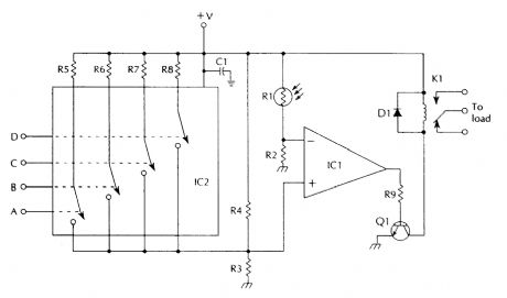
Digital inputs A, B, C, D select different light levels by varying the value of bridge circuit resis-tance R4.IC1 741 op ampIC2 CD4066 quad bilateral switchQ1 NPN transistor (2N2222, 2N3904, or similar) D1 diode (1N4002, or similar)C1 0.1-μF capacitorR1 photoresistorR2, R3 390-kΩ, 1/4-W 5% resistorR4, R5 1-MΩ, 1/4-W 5% resistorR6 820-kΩ, 1/4-W 5% resistorR7 470-kΩ, 1/4-W 5% resistorR8 270-kΩ, 1/4-W 5% resistorR9 100-kΩ, 1/4-W 5% resistorK1 relay to suit load (View)
View full Circuit Diagram | Comments | Reading(0)
TRAFFIC_LIGHT_CONTROLLER
Published:2009/6/22 22:49:00 Author:Jessie
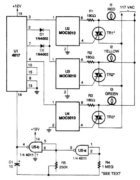
Oscillator U5A-B drives a 4017 divide-by-10 counter. The first output of U1 appears at pin 3, which supplies a positive voltage to U2, a MOO 3010 optocoupler/triac-driver IC, turning it and triac TR1 on. That lights I1, the red lamp. The second output appears at pin 2 and passes through D1 to the second MOC 3010, U3, thereby lighting the yellow lamp, I2. The third output at pin 4 turns on UJ4 and the green lamp, I3. The fourth output at pin 7 travels through D2 and into U3 to light the yellow lamp, I2, again.If you would like the traffic-light system to follow the normal sequence of green, yellow, and red, make the following circuit changes: Disconnect pins 10 and 15 of U1 from each other. Remove D1 and D2 and connect pin 2 of U1 to pin 1 of U3. Then connect pins 7 and pins 15 of UI together. Use U2 to drive I3 (the green light) and U4 for I1 (the red light). (View)
View full Circuit Diagram | Comments | Reading(3919)
ALARM_DIALER
Published:2009/6/22 22:48:00 Author:Jessie
This circuit dials a stored DTMF tone sequence from EPROM when a control line is taken to 0 V. IC1 is a Schmitt trigger oscillator, running at around 2 Hz. It clocks a 4024 binary counter. The coun-ter's outputs connect to the address leads of the EPROM. A 2716 was used here, but the choice of EPROM is by no means critical.Normally, the counter is held reset by a logic 1 on its reset pin (pin 2). When the trigger input is sent low, pin 10 of IC1 goes low, pin 3 goes high, and the reset is removed from the counter. It then begins to clock, incrementing the EPROM. When moved from address 000000, the data on bit DO of the EPROM changes to a logic 1 and holds the circuit running. The last address should have data 11111110 to reset the circuit to standby. (View)
View full Circuit Diagram | Comments | Reading(3599)
| Pages:177/312 At 20161162163164165166167168169170171172173174175176177178179180Under 20 |
Circuit Categories
power supply circuit
Amplifier Circuit
Basic Circuit
LED and Light Circuit
Sensor Circuit
Signal Processing
Electrical Equipment Circuit
Control Circuit
Remote Control Circuit
A/D-D/A Converter Circuit
Audio Circuit
Measuring and Test Circuit
Communication Circuit
Computer-Related Circuit
555 Circuit
Automotive Circuit
Repairing Circuit