
Index 64
FIELD_STRENGTH_METER
Published:2009/7/1 23:51:00 Author:May
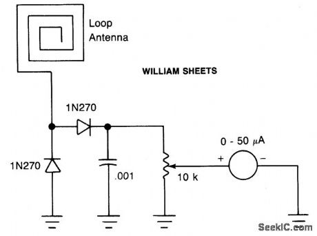
The antenna consists of about 20 cm of insulated stranded wire glued or taped around the inside of a small plastic box. RF current is rectified by two diodes, and a 10 k potentiometer provides variable attenuation for the meter. (View)
View full Circuit Diagram | Comments | Reading(0)
MOSFET_DIP_METER_
Published:2009/7/1 23:32:00 Author:May
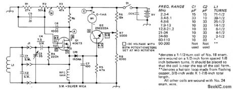
Output of groundeddrain Colpitts oscillator using RCA N-channel dual-gate MOSFETQ1 is detected by CR1 and amplified by Q2 for driving meter. Frequency of oscillation depends on C1, C2, C3, and L1, and reaches 250 MHz when L1 is reduced to hairpin.Table gives values of plug-in assembly L1-C1-C2 for nine frequency ranges. Circuit was designed for 12-V supply but works well with 9-V battery shown if drain resistor RD, is shorted. Battery drain is about 20 mA. All coils are wound on Millen 45004 forms.-F. Bruin, A Dual-Gate MOSFET Dip Meter, QST, Jan. 1977, p 16-17. (View)
View full Circuit Diagram | Comments | Reading(3008)
PULSE_RATE_DETECTOR
Published:2009/7/1 22:54:00 Author:May
Operates from 1 Hz to 2 MHz, providing one logic level when input rate crosses set point and opposite logic level when input rate falls below set point. Serpoint rate is reciprocal of MVBR time, or 1/R1C1.Two periods of input signal are sufficient for response to rate change. Value of C2 is R1C1/ 1.5x 10⁶.-J. M. Toth, Versatile Circuit Forms Accurate Pulse-Rate Detector, EDN Magazine, Aug. 20, 1977, p 142-143. (View)
View full Circuit Diagram | Comments | Reading(1048)
AF_METER_
Published:2009/7/1 22:32:00 Author:May
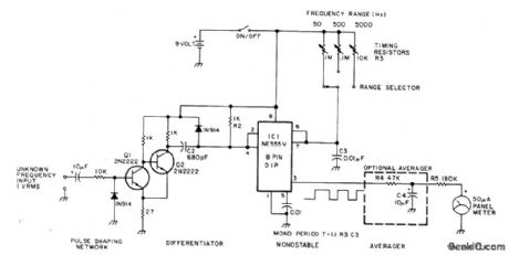
Timer IC1 forms basis for Iinearfrequency meter covering audio spectrum. Mono MVBR puts out fixed-width pulse when triggered by unknown inputfrequency. Article covers operation and calibration. Errata: pin 4 of 555 should be connected to pin 8 instead of to pin 2,-G.Hinkle,IC Audio IC Audio Frequency Meter,73 Magazine,Holiday issue 1976、p 61. (View)
View full Circuit Diagram | Comments | Reading(926)
NANOSECOND_PULSE_DETECTOR
Published:2009/7/1 22:31:00 Author:May
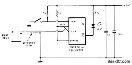
Used to provide visual indication of presence of a nonrepetitive digital pulse having microsecond or nanosecond width. Bistable IC transfers pulse information from its data input to the Q output on positive-going edge of clock pulse, to energize LED indicator.-P. V. Prior, Digital Pulse Detector, Wireless World, March 1976, p 90. (View)
View full Circuit Diagram | Comments | Reading(1147)
LIGHT_SENSITIVE_THEREMIN
Published:2009/7/1 22:23:00 Author:May
Tone of loudspeaker increases and decreases in frequency as flashlight is moved in vicinity of photocell in darkened room, Use Radio Shaok 276-116cadmium sulfide photocell. Cell resistance decreases with light, increasing frequency ot audio oscillator. Continuously changing frequency resembles that produced by hand-con-ttolled theremin.-F. M, Mims, Electronic Music Projects, Vol. l, 'Radio Shack, Fort Worth. TX. 1977. 2nd Ed., p 91-95. (View)
View full Circuit Diagram | Comments | Reading(1913)
FREQUENCY_METER_
Published:2009/7/1 22:21:00 Author:May
High- precision frequency-to-voltage converter can be used as frequency meter in laboratory. Input frequency range up to 1 kHz is converted to corresponding full-scale voltage value of +5 V. Two-pole filter removes ripple from positive output pulses across R1 before signal is fed to 3130 opamp that provides gain and zero adjustments.-W. G. Jung,″IC Timer Cookbook,″Howard W .Sams,Indianaplis,IN,1977,p 192-186. (View)
View full Circuit Diagram | Comments | Reading(1372)
CONTRAST_METER
Published:2009/7/1 21:28:00 Author:May
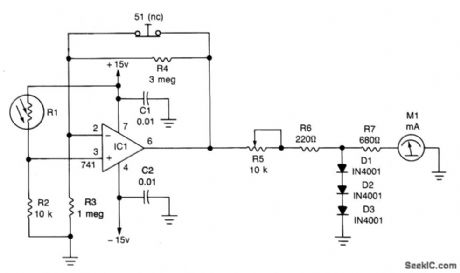
Circuit Notes
One leg of the photocell (R1) is tied to the +15 volt supply and the other end is connected to ground through resistor R2, forming a voltage-divider network. The noninverting input of the 741 op amp, IC1, is tied to the junction formed by R1 and R2, while its inverting input is grounded through resistor R3. When switch S1is pressed, another divider network is formed, reducing the voltage applied to the inverting input of the op amp. When light hits the photocell its resistance begins to decrease causing a greater voltage drop across R2 and a higher voltage to be presented to the non-inverting input of IC1. This causes IC1 to output a voltage proportional to the two inputs. The circuit gives a meter reading that depends on the intensity of light hitting photocell R1; therefore, R1 should be mounted in a bottle cap so that the light must pass through a 3/16 inch hole. Potentiometer R5 is used to adjust the circuit for the negative you're working with. (View)
View full Circuit Diagram | Comments | Reading(810)
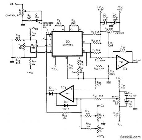
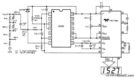
3_1_2_DIGIT_TRUE_RMS_AC_VOLTMETER
Published:2009/7/1 21:24:00 Author:May
View full Circuit Diagram | Comments | Reading(2888)
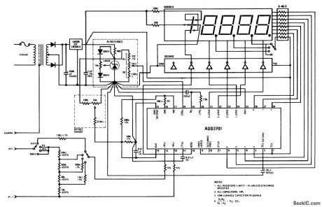
3_3_4_DIGIT_DVM_FOUR_DECADE_±04_V_±4_V_±40_V_AND±400_V_FULL_SCALE
Published:2009/7/1 21:21:00 Author:May
View full Circuit Diagram | Comments | Reading(960)
SHUTTER_SPEED_TESTER
Published:2009/7/1 21:20:00 Author:May
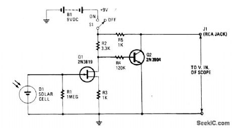
Circuit NotesThe soiar cell is connected across the input of the FET (fleld-effect transistor), Q1, so that it will produce positive dc voltage to the gate when activated by light shining through the open shutter, decreasing the negative gate-source bias already established by the source resistor, and causes an increase in drain current. The drain voltage goes more negative which causes a decrease in Q2's base current. Q2's collector current decreases, and its collector voltage becomes more positive. There is an amplified positive-going voltage output at the collector, and it's applied directly to the oscilloscope's vertical input, producing a waveform that is displaced vertically whenever light strikes the cell. (View)
View full Circuit Diagram | Comments | Reading(1162)
FREQUENCY_LIMIT_DETECTOR
Published:2009/7/1 21:15:00 Author:May
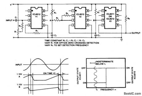
Simple frequency limit detectors providing a GO/NO-GO output for use with varying amplitude input signals may be conveniently implemented with the ICL8211/8212. In the application shown, the first ICL8212 is used as a zero-crossing detector. The output circuit consisting of R3, R4 and C2 results in a slow output positive ramp. The negative range is much faster than the positive range. R5 and Rg provide hysteresis so that under all circumstances the second ICL8212 is turned on for sufficient time to discharge C3.The time constant of R7C3 is much greater than R4C2. Depending upon the desired output polarities for low and high input frequencies, either an ICL8211 or an ICL8212 may be used as the output driver.The circuit is sensitive to supply voltage variations and should be used with a stabilized power supply. At very low frequencies the output will switch at the input frequency. (View)
View full Circuit Diagram | Comments | Reading(0)
PHASE_DETECTOR_WITH_10_BIT_ACCURACY
Published:2009/7/1 21:10:00 Author:May
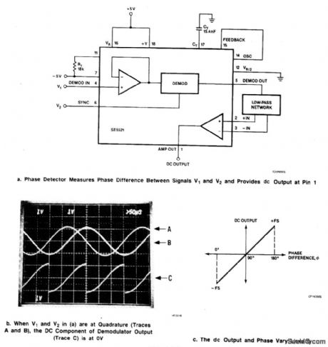
Signals of identical frequency are applied to sync input (Pin 6) and to the demodulator input (Pin 4), respectively, the demodulator functions as a phase detector with output dc component being proportional to phase difference between the two inputs. The signals must be referenced to 0 V for dual supply operation or to VR/2 for single supply operation.At ± 5-V supplies, the demodulator can easily handle 7-V peak-to-peak signals. The low-pass network configured with the uncommitted amplifier dc output at Pin 1 of the device. The dc output is maximum (+ full-scale) when V1 and V2 are 180°out of phase and minimum (- full-scale) when the signals are in phase. (View)
View full Circuit Diagram | Comments | Reading(1059)
TACHOMETER,SINGLE_PULSE_GENERATOR,POWER_LOSS_DETECTOR,PEAK_DETECTOR
Published:2009/7/1 21:06:00 Author:May
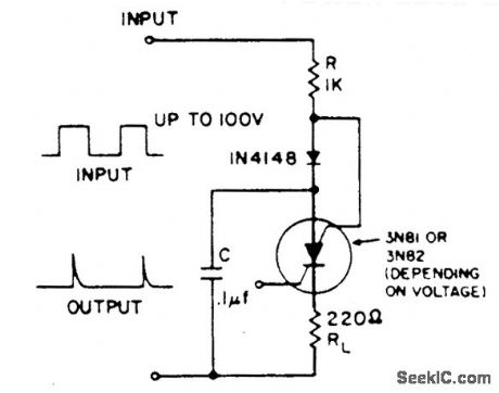
A positive going input charges C through the IN4148 and R. The diode keeps the scs off.A negative going input supplies anode-gate current triggering on the scs discharging C through RL. (View)
View full Circuit Diagram | Comments | Reading(1142)
HIGH_FREQUENCY_PEAK_DETECTOR
Published:2009/7/1 21:04:00 Author:May
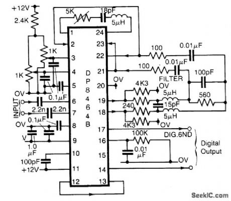
National Semiconductor's DP8464B is primarily intended for use in disk systems as a pulse detector. However it can be easily used as a general purpose peak detector for analogue signals up to 5 MHz. The chip can handle signals between 20 and 66 mV peak-to-peak. The circuit includes a filter with constant group delay characteristics to band limit the signal. Typically the -3 dB point for this filter will be at about 1.5 times the highest frequency of interest. This differentiator network between pins 1 and 24 can be as simple as a capacitor, or can be more complex to band limit the differentiator response. (View)
View full Circuit Diagram | Comments | Reading(911)
LEVEL_DETECTOR
Published:2009/7/1 21:00:00 Author:May

By using the ICL7612 in these applications, the circuits will follow rail to rail inputs. (View)
View full Circuit Diagram | Comments | Reading(0)
PEAK_DETECTOR
Published:2009/7/1 20:57:00 Author:May
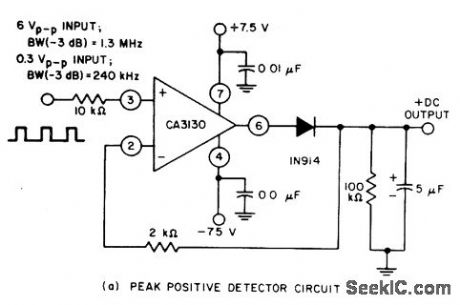
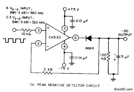
Circuits are easily implemented using the CA3130 BiMOS op amp. For large-signal inputs the bandwidth of the peak-negative circuit is less than that of the peak-positive circuit. The second stage of the CA3130 limits bandwidth in this case. (View)
View full Circuit Diagram | Comments | Reading(3355)
ZERO_CROSSING_DETECTOR
Published:2009/7/1 20:49:00 Author:May
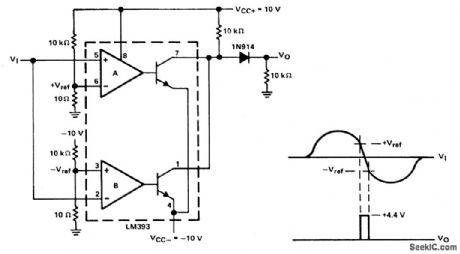
This zero-crossing detector uses a dual LM393 comparator, and easily controls hysteresis by the reference levels which are set on the comparator inputs. The circuit illustrated is powered by ±10-V power supplies. The input signal can be an ac signal level up to + 8 V. The output will be a positive going pulse of about 4.4 V at the zero-crossover point. These parameters are compatible with TTL logic levels.The input signal is simultaneously applied to the non-inverting input of comparator A and the inverting input of comparator B. The inverting mput of comparator A has a + 10 mV reference with respect to ground, while the non-inverting input of comparator B has a -10 mV reference with respect to ground. As the input signal swings positive (greater than +10 mV), the output of comparator A will be low while comparator B will have a high output. When the input signal swings negative (less than - 10 mV), the reverse is true. The result of the combined outputs will be low in either case. On the other hand, when the input signal is between the threshold points (±10 mV around zero crossover), the output of both comparators will be high. If more hysteresis is needed, the ±10 mV window may be made wider by increasing the reference voltages. (View)
View full Circuit Diagram | Comments | Reading(2)
VOLTAGE_LEVEL_DETECTOR
Published:2009/7/1 20:44:00 Author:May
View full Circuit Diagram | Comments | Reading(799)
PULSE_SEQUENCE_DETECTOR
Published:2009/7/1 20:42:00 Author:May
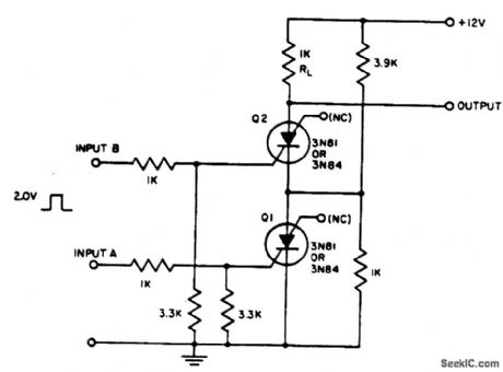
The resistor divider connected between Q1and Q2 supplies IH to Q1 after input A triggersit. It also prevents input B from triggering Q2until Q1 conducts. Consequently, the first Binput pulse after input A is applied will supply current to RL. (View)
View full Circuit Diagram | Comments | Reading(0)
| Pages:64/101 At 206162636465666768697071727374757677787980Under 20 |
Circuit Categories
power supply circuit
Amplifier Circuit
Basic Circuit
LED and Light Circuit
Sensor Circuit
Signal Processing
Electrical Equipment Circuit
Control Circuit
Remote Control Circuit
A/D-D/A Converter Circuit
Audio Circuit
Measuring and Test Circuit
Communication Circuit
Computer-Related Circuit
555 Circuit
Automotive Circuit
Repairing Circuit