
Index 60
MISSING_PULSE_DETECTOR
Published:2009/7/6 2:36:00 Author:May
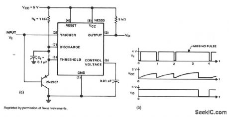
This circuit will detect a missing pulse or abnormally long spacing between consecutive pulses in a train of pulses. The timer is connected in the monostable mode. The time delay should be set slightly longer than the timing of the input pulses. The timing interval of the monostable circuit is continuously retriggered by the input pulse train, VI. The pulse spacing is less than the timing interval, which prevents VC from rising high enough to end the timing cycle. A longer pulse spacing, a missing pulse, or a termi-nated pulse train will permit the timing interval to be completed. This will generate an output pulse, VO as illustrated in Fig. 25-3b. The output remains high on pin 3 until a missing pulse is detected at which time the output decreases.
The NE555 monostable circuit should be running slightly slower, lower in frequency, than the frequency to be analyzed. Also, the input cannot be more than twice this free-running frequency or it would retrigger before the timeout and the output would remain in the low state continuously. The circuit oper-ates in the monostable mode at about 8 kHz, so pulse trains of 8 to 16 kHz can be observed. (View)
View full Circuit Diagram | Comments | Reading(0)
DIGITAL_FREQUENCY_DETECTOR
Published:2009/7/6 2:32:00 Author:May
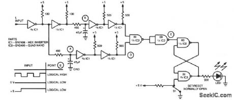
A simple inventer and NAND gate can be connected to yield a highly compact and reliable digital frequency detector. This circuit can detect frequencies up to 3 MHz with 50% duty cycles. When a frequency, fi, appears at the input, points A and B detect a logical high dc level. Thereupon point E increases the latch sets and the LED lights. If the input frequency is absent and if the voltage is either at a constant high or low level, points A and B will be complementary and point E will decrease. This will reset the latch and extinguish the LED. (View)
View full Circuit Diagram | Comments | Reading(2224)
HALF_WAVE_RECTIFIER
Published:2009/7/6 2:24:00 Author:May
Circuit Notes
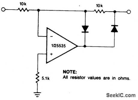
The circuit provides for accurate half-wave rectification of the incoming signal. For positive signals, the gain is 0; for negative signals, the gain is -1. By reversing both diodes, the polarity can be inverted. This circuit provides an accurate output, but the output impedance differs for the two input polarities and buffering may be needed. The output must slew through two diode drops when the input polarity reverses. The NE5535 device will work up to 10 kHz with less than 5% distortion. (View)
View full Circuit Diagram | Comments | Reading(0)
OUT_OF_BOUNDS_PULSE_WIDTH_DETECTOR
Published:2009/7/6 2:24:00 Author:May
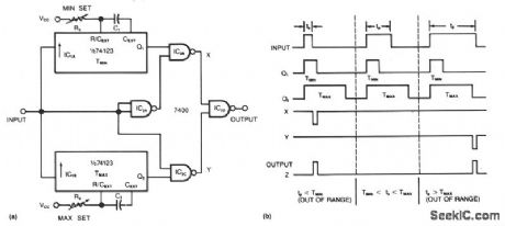
Requiring only two ICs to monitor a train of positive pulses, this circuit produces a single positive output pulse for each input pulse whose duration is either too long or too short. You specify the minimum and maximum limits by adjusting the trimming potentiometers, R1 and R2. You can set the value of the acceptable pulse width from approximately 50 ns to 10 μs, for a 74123 monostable multivibrator. The leading edge of an input pulse triggers one shots ICIA and ICIB as you can see from the timing diagram. Each NAND-gate output is high unless either or both inputs are low, so outputs X and Y are high unless the circuit encounters an out-of-range pulse. IC2D then gates a negative pulse from IC2B or IC2C to produce the circuit's positive output pulse. (View)
View full Circuit Diagram | Comments | Reading(1255)
EDGE_DETECTOR
Published:2009/7/6 2:16:00 Author:May
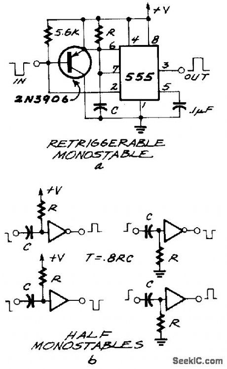
The 555 is a monostable that wants a negative-going trigger. If the pulse you're feeding it with is positive-going, you can run it through an inverter made up of either an inverting gate or, if you're tight on space, a single transistor. Both ways are shown. The circuits shown in Fig. 25-9b are edge detectors as well, and are usually referred to as half monostables, since they can't be used in every application. The width of the output pulse is deter-mined by the RC value, but there are a few rules governing their use:
.The input pulse has to be wider than the output pulse.The input pulse can't be glitchy. The circuit can't be retriggered faster than the RC time (View)
View full Circuit Diagram | Comments | Reading(0)
RECEIVER_MONITOR
Published:2009/7/6 2:13:00 Author:May
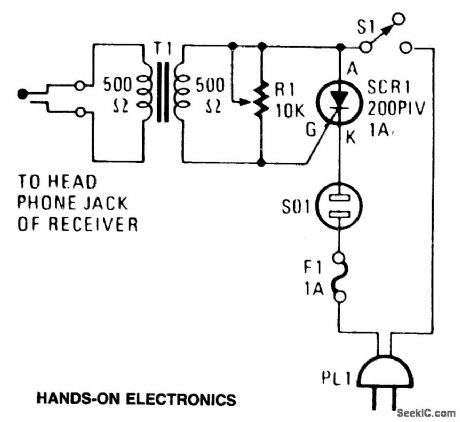
Circuit Notes
The alarm plugs into the earphone jack on a receiver. Then when a signal (normally fed to the headphones) is detected and applied to the gate of SCR1, it conducts, sounding whatever alarm is connected to SO1. The signaling device can be an audible alarm or a lamp. Variable resistor R1 functions as a sensitivity control so that background noises won't trigger the alarm. (View)
View full Circuit Diagram | Comments | Reading(859)
LOW_DRIFT_PEAK_DETECTOR
Published:2009/7/6 2:13:00 Author:May
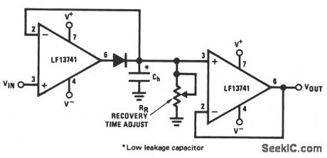
This circuit uses op amp U1 to compensate for the offset in peak detector diode D1. Across Ch is the exact peak voltage; U2 is used as a voltage follower to read this voltage. (View)
View full Circuit Diagram | Comments | Reading(0)
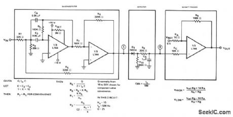
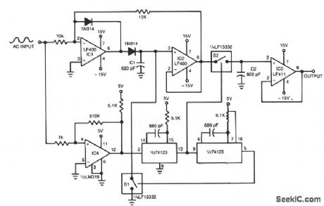
FREQUENCY_BOUNDARY_DETECTOR
Published:2009/7/6 2:09:00 Author:May
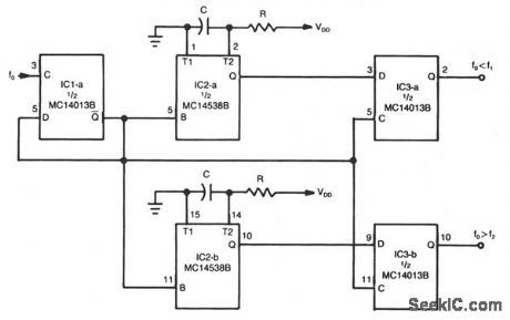
The circuit can be used to tell whether or not an input signal is within a certain frequency range. The device consists of three ICs, a dual monostable multivibrator, and two dual D-type flip-flops. The signal whose frequency is in question is fed to the clock input of one of the flip-flops. The Q output of that flip-f1op (IC1a) is cross coupled to its data input so that it acts like a divide-by-two counter. The trailing edge of the Q output is used to trigger the one shots formed by IC2. The upper- and lower-frequency boundaries are determined by the two sections of IC2 ; the dual precision monostable multivibrator and their external rc networks. The upper-frequency boundary, f1, is set by the output of IC2a, and the lower-frequency boundary, f2, is set by the output of IC2b.
The frequency of the input to the circuit can be anywhere from dc to 100 kHz. The states of the out-puts of IC2, which determine the upper- and lower-frequency boundaries, are latched by IC3a and IC3b respectively. The output of IC3a will be high only when the input frequency is less than that of the output of IC2a, f1 The output of IC3b will be high only when the frequency of the input is greater than that of the output of IC2b, f2. (View)
View full Circuit Diagram | Comments | Reading(934)
PRECISION_ENVELOPE_DETECTOR
Published:2009/7/6 2:02:00 Author:May
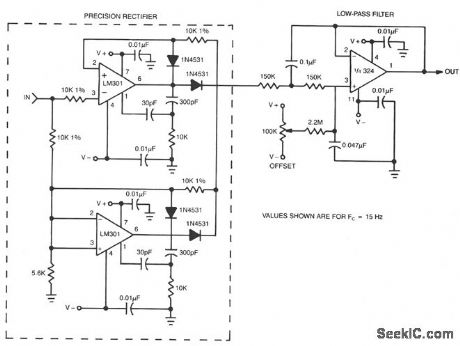
This circuit is useful for signal-processing sonar data recorded on an instrumentation-quality analog tape recorder. The envelope detector utilizes ready available parts, and furnishes accuracy beyond 100 kHz. Two LM301 op amps connected as precision absolute-value circuits use 2-pole frequency compensa-tion for increased slew rate. And one section of an LM324 quad op amp connected in a Butterworth LPF configuration subjects the rectifier's output to a low-pass filter. (View)
View full Circuit Diagram | Comments | Reading(2401)
AUDIO_DECIBEL_LEVEL_DETECTOR_WITH_METER_DRIVER
Published:2009/7/6 1:58:00 Author:May
This circuit draws very little power, less than 5 mA with a single 6-V power supply, making it ideal for portable battery-operated equipment. The small size and low power consumption belie the 90-dB dynamic range and 10.5-μV sensitivity. Dc output voltage proportional to the log10 of the input signal level. Thus, a standard 0-5 voltmeter can be linearly calibrated in decibels over a single 80-dB range. The circuit is within 1.5-dB tolerance over the 80-dB range for audio frequencies from 100 Hz to 10 kHz. Higher audio levels can be measured by placing an attenuator ahead of the input capacitor. (View)
View full Circuit Diagram | Comments | Reading(1533)
RADAR_SIGNAL_DETECTOR
Published:2009/7/6 1:54:00 Author:May
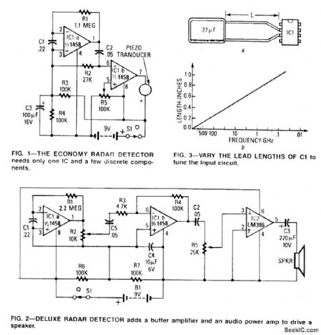
Circuit Notes
The circuit can be tuned to respond to signals between 50 MHz and 500 GHz. The economy model is shown in Fig. 1, and the deluxe model is shown in Fig. 2. The ftrst op amp in each circuit functions as a culrent-to-voltage converter. In the economy model IC1b buffers the output to drive the piezo buzzer. The deluxe model functions in a similar manner except that IC1b is configured as a x20 buffer amplifier to drive the LM386. In both circuits C1 functions as a transmission line that intercepts the incident radar signal. The response may be optimized by trimming C1's lead length for the desired frequency. Typically the capacitor's leads should be 0.5-0.6 inches long. (View)
View full Circuit Diagram | Comments | Reading(1499)
500_Hz_TONE_DETECTOR
Published:2009/7/6 1:50:00 Author:May
View full Circuit Diagram | Comments | Reading(791)
ONE_CHIP_RADAR_DETECTION_CIRCUIT
Published:2009/7/6 1:48:00 Author:May
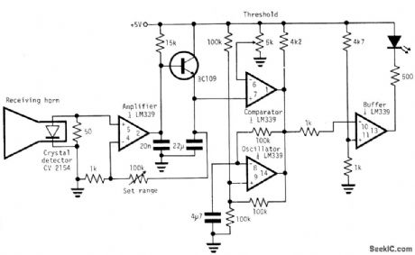
Circuit Notes
A simple X-band. radar detector is capable of indicating changes in rf radiation strength at levels down to 2 mW/cm2. Radiation falling on the detector diode, produces a voltage at the input of an amplifter whose gain may be adjusted to vary the range at which the warning is given. The amplifier output drives a voltage comparator with a variable threshold set to a level that avoids false alarms. The comparator output is connected in the wired-OR configuration with the open collector output of an oscillator running at a frequency of 2 Hz. In the absence of a signal, the comparator output level is low, inhibiting the oscillator output stage and holding the buffer so the lamp is off. When a signal appears, the comparator output goes high, removing the lock from the oscillator which free-runs, switching the lamp on and off at 2 Hz. (View)
View full Circuit Diagram | Comments | Reading(4698)
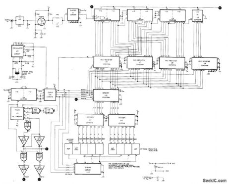
12_V_5_MHz_COUNTER
Published:2009/7/6 1:48:00 Author:May
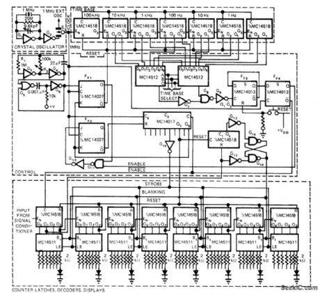
Portable counter is designed with low-power logic to minimize battery drain, yet provides good performance.Since most of milliwatt power drain is taken by digital readout, circuit blanks out LED display when there is no input signal. Time base divides 1-MHz crystal oscillator frequency down to desired enable time, up to tOs, using 31/2 MC14518 dual decade counters connected in ripple-through mode. Actual counting of input signal codes is also done with MC14518 counters.Latches and BCD to 7-segment decoders use MC14511s. Enable line tums first counter on and off for precise enable time period. Strobe line transfers count into memory of MC14511 latch decoder, and control line resets MC14518 decade counters for next count cycle. Displays are Monsanto MAN-4 LEDs. Article traces circuit operation in detail and gives timing diagram.-D. Aldridge, CMOS Counter Circuitry Slashes Battery Power Requirements, EDN Magazine, Oct. 20, 1974, p 65-71.
(View)
View full Circuit Diagram | Comments | Reading(2603)
ANALOG_PEAK_DETECTOR_WITH_DIGITAL_HOLD
Published:2009/7/6 1:46:00 Author:May
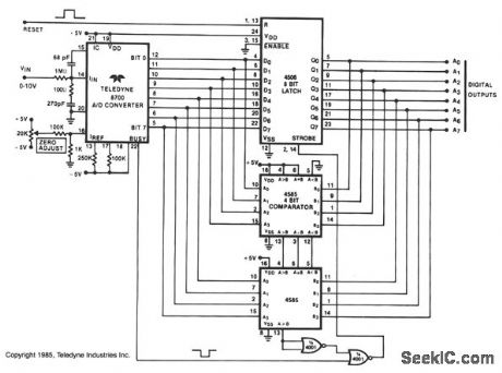
Analog peak detection is accomplished by repeatedly measuring the input signal with an a/d converter and comparing the current reading with the previous reading. If the current reading is larger than the previous, the current reading is stored in the latch and becomes the new peak value. Since the peak is stored in a CMOS latch, the peak can be stored indefinitely. (View)
View full Circuit Diagram | Comments | Reading(1387)
WIDE_RANGE_PEAK_DETECTOR
Published:2009/7/6 1:41:00 Author:May
IC1 and IC2 form an inverting half-wave precision-rectifter/peak-detector circuit. Negative input-signal, swings with peaks larger than the voltage on C1, cause this capacitor to charge to the new peak voltage. The capacitor holds this voltage until a larger signal peak arrives. When the input swings high, comparator IC4 detects the zero crossing and triggers the one-shot multivibrator. The one shot closes FET switch S2, thereby causing C2 to charge to the peak voltage held on C1, during the previous half cycle. The second one shot then produces a pulse that causes FET switch S1 to discharge C1. If the next negative signal-input peak is different from the previous one, the circuit captures it and it appears at 1C3's output during the next half cycle. The peak detector thus resets itself once every input-waveform cycle. Note that the zero crossings are necessary to trigger the switches; therefore, the circuit is usable only with ac signals. (View)
View full Circuit Diagram | Comments | Reading(1907)
PLL_WITH_IC_TIMER
Published:2009/7/6 1:18:00 Author:May
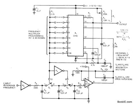
Uses 2240 programmable timer/counter as combination voltage-con-trolled oscillator and frequency divider, with CMOS analog switches serving as sample-and-hold phase detectors. Incoming reference frequency is amplified and limited by CMOS inverter, then integrated into reference triangle waveform by R9-C2. Triangle is sampled by S1 and S2 whieh with CH1 and CH2 form cascaded sample-and-hold network that holds only last instantaneous voltage on CH1 as error voltage. This error is amplified by FET-input 3140 opamp A2 for driving pin 12 of 2240 timer as correction voltage, to establish lock. Reference and output frequencies need not have direct harmonic (View)
View full Circuit Diagram | Comments | Reading(1919)
LOSS_OF_LOCK_MONITOR
Published:2009/7/6 1:10:00 Author:May
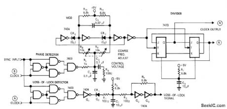
Modified digital phase-locked loop includes second phase detector that provides alarm signal when loop gets out of lock. Output may also be used to disable other circuits. Voltage-controlled multivibrator VCO, operating at 4 times desired clock frequency, drives two-stage switch-tailed ring counter that provides two-phase internal clock signals A and B for detectors. Article descirbes operation of circuit and give timing digrams.-C.A. Herbst, Digital Phase-Locked Loop with Loss-of-Lock Monitor, EDN|EEE magazine, Oct. 15, 1971, p, 64-65. (View)
View full Circuit Diagram | Comments | Reading(2573)
100_Hz_TO_1_MHz_PHASE_METER
Published:2009/7/6 1:08:00 Author:May
Provides better than 2% accuracy over most of frequency range, as required for making Bode plots. Based on squaring two sine waves and comparing amount of overlap to total period of an input wave. This gives directly the amount of phase difference between input wave trains, up to 180°. Instead of measuring periods, overlap is integrated over total period to give average of ON to OFF times that can be read as phase difference on voltmeter. Article gives erformancespecifications and describes circuit operation in detail.-D. Kesner, IC Phase Meter Beats High Costs, EDN|EEE Magazine, Oct. 15, 1971, p 49-52. (View)
View full Circuit Diagram | Comments | Reading(943)
4_MHz_COUNTER
Published:2009/7/5 23:59:00 Author:May
Portable frequency counter using RCA CMOS logic draws only 300 mW (12 V at 25 mA) yet operates to well above 4 MHz.Supply voltage can be between 4 and 15 V, loosely regulated, without affecting accuracy.Display uses multiplexing with 10% duty cycle to minimize battery drain. One multiplexed output is for three least signmcint figures and other for four most significant figures. Article describes operation in detail. Applications in.dude setting RTTY mark and space tones, FM repeatertones, signal-generator frequencies for TV alignment, tuning musical instruments, and serving as tachometer or speedometer in car.-R. M. Mendelson, Milliwatt Portable Counter, Ham Fladio, Feb. 1977, p 22-25.
(View)
View full Circuit Diagram | Comments | Reading(1829)
| Pages:60/101 At 204142434445464748495051525354555657585960Under 20 |
Circuit Categories
power supply circuit
Amplifier Circuit
Basic Circuit
LED and Light Circuit
Sensor Circuit
Signal Processing
Electrical Equipment Circuit
Control Circuit
Remote Control Circuit
A/D-D/A Converter Circuit
Audio Circuit
Measuring and Test Circuit
Communication Circuit
Computer-Related Circuit
555 Circuit
Automotive Circuit
Repairing Circuit