
Index 59
AUTO_BATTERY_ALTERNATOR_MONITOR
Published:2009/7/6 5:38:00 Author:May
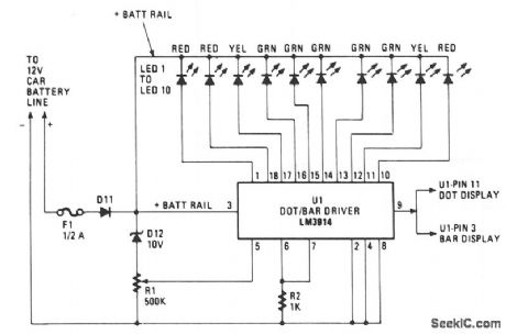
Most of the circuitry is contained in the LM3914 dot/bar-graph driver IC chip. In addition to the comparator circuitry within the package, it also contains a stable reference supply and the driv-ers for the LEDs. Resistor R2 acts as the current limiter for all the LEDs. Resistor R2 may be varied for LED brightness.
The unit will illuminate one LED for each volt-age condition encountered in the charging system.This system is called a dot-graph display; it is achieved by wiring the mode control at pin 9 to pin 11 on U1.
It is possible to wire the monitor so that each lamp will be illuminated up to the maximum voltage on the line at that moment. The latter is referred to as a bar-graph display. By connecting pin 9 to pin 3 on U1, the bar-graph mode will be enabled. (View)
View full Circuit Diagram | Comments | Reading(2471)
LINE_DROPOUT_DETECTOR
Published:2009/7/6 5:30:00 Author:May
View full Circuit Diagram | Comments | Reading(768)
ACCURATE_DIGITAL_CAPACITANCE_METER
Published:2009/7/6 5:20:00 Author:May
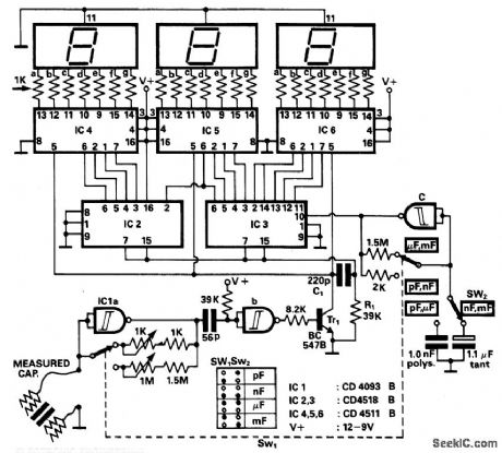
The principle of operation is counting the pulse number derived from a constant frequency oscillator during a fixed time interval produced by another lower frequency oscillator. This oscillator uses the capacitor being measured as the timing. The capacitance measurement is proportional during pulse counting during a fixed time interval. The astable oscillator formed by IC1c produces a pulse train of constant frequency. Gate IC1a also forms an oscillator whose oscillation period is given approximately by the equation: T=0.7 RC. Period T is linearly dependent on the capacitance C. This period is used as the time interval for one measurement. The differentiator network following the oscillator creates the negative spikes shaped in narrow pulses by IC1b NAND Schmitt Trigger. The differentiator formed by R1 and C1 produces a negative spike which resets the counters.The display shows the number of high frequency oscillator pulses entering the counter during the measurement period. (View)
View full Circuit Diagram | Comments | Reading(2801)
FIELD_STRENGTH_METER
Published:2009/7/6 5:13:00 Author:May
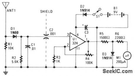
The untuned, but amplified FSM can almost sense that mythical flea's whisper-from 3 through 148 MHz no less-and yet, is so immune to overload that the meter pointer won't pin. The key to the circuit is the amplifter, a 324 quad op amp, of which only one section is used. It's designed for a single-ended power supply, will provide at least 20-dB dc gain, and the output current is self-limiting. The pointer can't be pinned. (View)
View full Circuit Diagram | Comments | Reading(0)
CAPACITANCE_TO_VOLTAGE_METER
Published:2009/7/6 5:09:00 Author:May

Timer U1 operates as a free-running oscillator at 60 Hz, providing trigger pulses to timer U2 which operates in the monostable mode. Resistor R1 is fixed and capacitor Cx is the capacitor being measured. While the output of U2 is 60 Hz, the duty cycle depends on the value of Cx. U3 is a combination low-pass filter and unity-gain follower whose dc voltage output is the time-averaged amplitude of the output pulses of U2, as shown in the timing diagram.
The diagram shows when the value of Cx is small the duty cycle is relatively low. The output pulses are narrow and produce a lower average dc voltage level at the output of U3. As the capacitance value of Ox increases, the duty cycle increases making the output pulses at U2 wider and the average dc level output at U3 increases. The graph illustrates capacitance values of 0.01 pF to 0.1 μF plotted against the output voltage of U3. Notice the excellent linearity and direct one-to-one scale calibration of the meter. If this does not occur the 100 k ohm resistor, R1, can be replaced with a potentiometer which can be adjusted to the proper value for the meter being used. (View)
View full Circuit Diagram | Comments | Reading(939)
LEAD_ACID_LOW_BATTERY_DETECTOR
Published:2009/7/6 4:32:00 Author:May
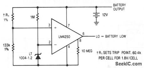
View full Circuit Diagram | Comments | Reading(774)
BATTERY_MONITOR
Published:2009/7/6 4:32:00 Author:May
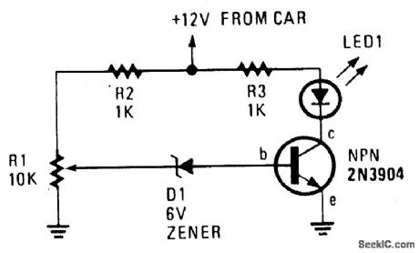
The circuit is quick and easy to put together and install, and tells you when battery voltage falls below the set limit as established by R1 (a 10,000-ohm potentiometer). It can indicate, via LED1, that the battery may be defective or in need of change if operating the starter causes the battery voltage to drop below the present limit. (View)
View full Circuit Diagram | Comments | Reading(0)
BATTERY_VOLTAGE_MONITOR
Published:2009/7/6 4:31:00 Author:May
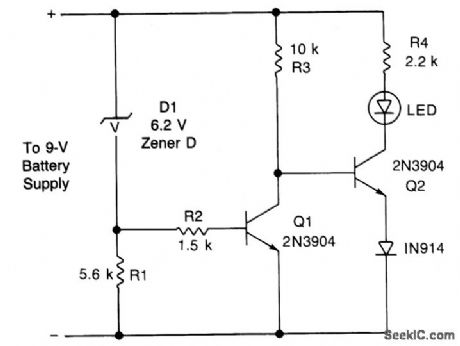
This circuit gives an early warning of the discharge of batteries. Zener diode D1 is chosen for the voltage below which an indication is required (9 V). Should the supply drop to below 7 V, D1 will cease conducting causing Q1 to shut off. Its collector voltage will now increase causing Q2 to start conducting via LED1 and its limiting resistor R4. (View)
View full Circuit Diagram | Comments | Reading(0)
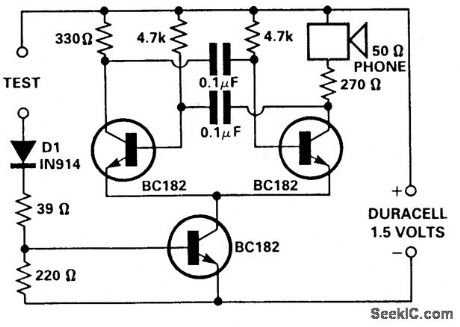
ADJUSTABLE,AUDIBLE_CONTINUITY_TESTER_FOR_DELICATE_CIRCUITS
Published:2009/7/6 3:54:00 Author:May
Circuit Notes
The tester gives an audible indication, making it unnecessary for the user to look directly at the instrument to observe a meter reading. In addition, the current and voltage of the tester are strictly limited. It can apply no more than 0.6 volts dc and no more than 3 mA through the probes. It can therefore be used safely on circuit boards in which semiconductor components have been installed, and on complementary metal oxide/semiconductor integrated circuits, which are highly susceptible to damage during testing. The tester can be adjusted to indicate continuity below any resistance value up to 35 ohms. For example, if the user sets the tester to 30 ohms, the unit will emit an audible tone whenever the resistance between the probes is 30 ohms or less; if, for example, the resistance is 30.2 ohms, the unit will remain silent. (View)
View full Circuit Diagram | Comments | Reading(1305)
SIMPLE_CONTINUITY_TESTER
Published:2009/7/6 3:51:00 Author:May

Circuit Notes
The pitch of the tone is dependent upon the resistance under test. The tester will respond to resistance of hundreds of kilohms, yet it is possible to distinguish differences of just a few tens of ohms in low-resistance circuits. Q1 and Q2 form a multivibrator, the frequency of which is infiuenced by the resistance between the test points. The output stage Q3 and Q4 will drive a small loudspeaker or a telephone earpiece. (View)
View full Circuit Diagram | Comments | Reading(2033)
SIMPLE_CONTINUITY_TESTER_FOR_PCBs
Published:2009/7/6 3:49:00 Author:May
Circuit NotesThis tester is for tracing wiring on Printed Circuit Boards. Resistors below 50 ohms act as a short circuit; above 100 ohms as an open circuit. The circuit is a simple multivibrator switched on by transistor T3. The components in the base of T3 are D1, R1, R2, and the test resistance. With a 1.5 volt supply, there is insufftcient voltage to turn on a semiconductor connected to the test terminals. (View)
View full Circuit Diagram | Comments | Reading(1944)
POSITIVE_PEAK_DETECTOR
Published:2009/7/6 3:45:00 Author:May
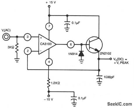
This peak detector uses a CA3100 BiMOS op amp as a wide-band noninverting amplifier to provide essentially constant gain for a wide range of input frequencies. The IN914 clips the negative half of VIN (R4)/(R3) (R5). A 500-μA load current is constant for all load values and the output reflects only positive input peaks. (View)
View full Circuit Diagram | Comments | Reading(0)
MULTIPLYING_D_A_CONVERTER
Published:2009/7/6 3:40:00 Author:May


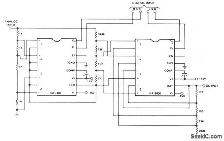
The circuit performs the function:
VOUT = VIN × N/16
where N IS the binary number from 0 to 15 formed by the digital input If the analog input iS a fixed dc reference,the circuit 15 a conventional 4-bit D to ac signal,in which case the output is the product of the analog signal and the digital signal The circuit on the left is a programmable attenuator with weights of 0,1/4,1/2,or 3/4 The circult on the rightis a noninverUng adder, which adds weights to the first output of 0,1/16,1/8,or 3/16 If four quadrant multiplicatlon is required,place a phase selector circuit in series with either the analog input or output The Do input of that stage becomes the+or-slgn bit of the atgttal input. (View)
View full Circuit Diagram | Comments | Reading(765)
DIRECTIONAL_SIGNALS_MONITOR
Published:2009/7/6 3:33:00 Author:May
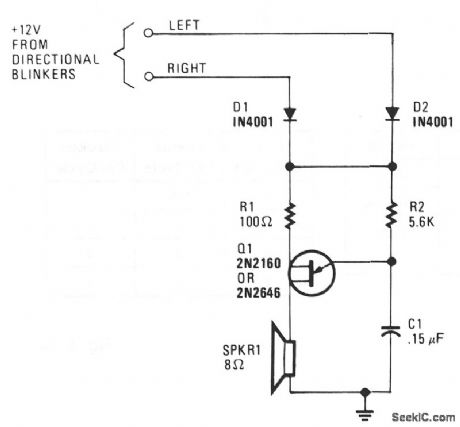
A unijunction transistor audio oscillator drives a small speaker. The oscillator's frequency is determined by resistor R2 and capacitor C2. The operating voltage is supplied from the car's turn-signal circuit(s) through D1 and D2. The diodes conduct current from the blinker circuit that is energized, and prevent stray current flow to the other blinker circuit. (View)
View full Circuit Diagram | Comments | Reading(1529)
PROGRAMMABLE_COUNTER
Published:2009/7/6 3:23:00 Author:May
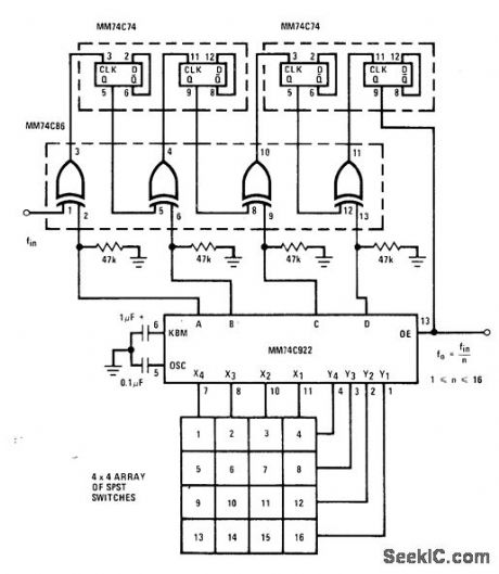
Input frequency can be divided by any number between 1 and 16 by pressing appropriate key on keyboard connected to National MM74C922 16-key encoder. Output frequency is symmetrical for odd and even divisors. Can be used for simple frequency synthesis or as keyboard-controlled CRO trigger. Operates over standard CMOS supply range of 3-15 V. Typical upperfrequency limit is 1 MHzwith 10-V supply. Circuit uses two MM74C74 dual D flip-flops and MM74C86 EX-CLUSIVE-OR package.- CMOS Databook, National Semiconductor, Santa Clara, CA, 1977, p 5-50-5-51.
(View)
View full Circuit Diagram | Comments | Reading(2229)
DOOR_AJAR_MONITOR
Published:2009/7/6 3:15:00 Author:May
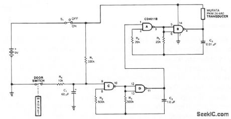
The monitor senses an ajar door and, if the situation isn't corrected within 20 seconds, sounds a beeping alarm. The circuit is controlled by a magnetic reed switch and magnet on the door. With the door closed, the switch is closed and the alarm is disarmed. Opening the door opens switch, C1 starts charging up through R1. Approximately 20 seconds later, the voltage at pin 9 is high enough to turn on the oscillator formed from C, D, R2, R3, and C2. That pulses the piezoelectric transducer's 3-kHz oscillator. For lower standby drain on the battery, change RI to 66 MO and C1 to 1 mF (film). (View)
View full Circuit Diagram | Comments | Reading(1849)
DIGITAL_TACH_DWELL_METER
Published:2009/7/6 3:10:00 Author:May
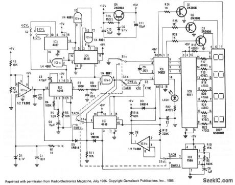
The heart of the circuit is IC2, a 4046 micropower phase-locked loop (PLL). The incoming signals are fed to the PLL after being buffered by IC1a and its associated components. The frequency of the incoming signal is multiplied by either 90, 60, or 45, depending on the setting of the cylinder select switch, S2. That switch selects the proper output from counters IC3 and IC4, which are set to divide the output frequency of the PLL by those amounts, and then send the divided output back to the comparator to the PLL to keep it locked on to the input signal. The phase pulses output at pin 4 of IC2, then go through an AND gate IC5d-which only passes the signals if the PLL is locked on to an input signal, preventing stray readings-and then to the input of IC6. When in the tach mode, IC6 counts the number of pulses present at pin 12, during the timing interval generated by IC8 and the associated circuitry of IClb. Because of the varied multiplication rate for the different cylinder selections-90, 60, and 45 for 4, 6, and 8 cylinders, respectively, the time interval is always constant at 1/3 of a second. The time interval is adjusted with R9, a 500-KΩ potentiometer; it is the only adjustment in the circuit.
In the high-tach (TACH 1 or x 100) range of 0- 9990 rpm, the output of IC2 is routed by switches S1a and S3 through IC7, a divide-by-ten counter, which increases the count range tenfold. In the low-tach (TACH 2 or x 10) range of 0- 999 rpm, the counter is bypassed.
(View)
View full Circuit Diagram | Comments | Reading(2102)
NULL_DETECTOR
Published:2009/7/6 2:52:00 Author:May
In this indicating comparator circuit, R2 setsthe hysteresis,If the 741 saturates at ±12 V. the current in R1 will be approximately±10 mA if 0.1 V hysteresis iS desired,Then 0.1 V/10 mA=10Ω=R2. (View)
View full Circuit Diagram | Comments | Reading(3130)
HIGH_BANDWIDTH_PEAK_DETECTOR
Published:2009/7/6 2:48:00 Author:May
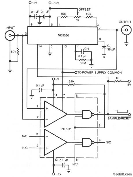
The high-speed peak detector uses a highly accurate, fast s/h amplifter controlled by a highspeed comparator. The s/h amplifter holds the peak voltage, until the comparator switches the amp to its sample mode, to capture a new, higher voltage level. The circuit handles all common-wave shapes and exhibits 5% accuracy from 50 Hz to 2 MHz.
The comparator's output decreases when the input signal exceeds the value of the currently held output. This transition puts the s/h amplifter into sample mode. Once the output reaches the value of the input, or the input signal falls below the output's level, the comparator's output increases; the high output brings the s/h amplifter back to the hold mode, thereby holding the peak value of the input signal. Reset the circuit by lowering the value of pin 4 of the NE522 comparator, which in turn allows the NE5060 s/h amplifter to acquire the input. The NE522 comparator has an open-collector output. (View)
View full Circuit Diagram | Comments | Reading(1327)
DIGITAL_PEAK_DETECTOR
Published:2009/7/6 2:44:00 Author:May
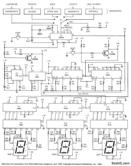
The peak detector tracks and holds, using the charge-storing ability of a capacitor, the highest output voltage from a transducer. Initially, the voltage on the inverting input of the comparator is at ground level. As a small voltage (0- 5 V) is captured by the peak detector and presented to the comparator's noninverting input, the output will swing high, which assets the bilateral switch; clock pulses now pass through the switch to clock both the BCD and binary counters. The outputs of the binary counters are connected to an R2R ladder network, which functions as a digital-to-analog converter. As the binary count increases, the R2R ladder voltage also increases until it reaches a point slightly above the voltage of the peak detector; at that instant, the comparator output swings low, which disables the bilateral switch and stops the counters.The number displayed on the 7-segment LED's vgill represent a value equivalent to the transducer's output. (View)
View full Circuit Diagram | Comments | Reading(1480)
| Pages:59/101 At 204142434445464748495051525354555657585960Under 20 |
Circuit Categories
power supply circuit
Amplifier Circuit
Basic Circuit
LED and Light Circuit
Sensor Circuit
Signal Processing
Electrical Equipment Circuit
Control Circuit
Remote Control Circuit
A/D-D/A Converter Circuit
Audio Circuit
Measuring and Test Circuit
Communication Circuit
Computer-Related Circuit
555 Circuit
Automotive Circuit
Repairing Circuit