
Index 41
LOG_ATTENUATOR_FOR_POSITIVE_PULSES
Published:2009/7/17 2:25:00 Author:Jessie
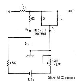
Output is proportional to log of input voltages between 0.1 and 100 V.-C. D. Nail, Logarithmic Attenuator Spans Three Decades, Electronics, 36:46, p 47-48. (View)
View full Circuit Diagram | Comments | Reading(863)
R_F_TRANSMITTER_POWER_AND_VSWR_MONI_TOR
Published:2009/7/17 2:24:00 Author:Jessie
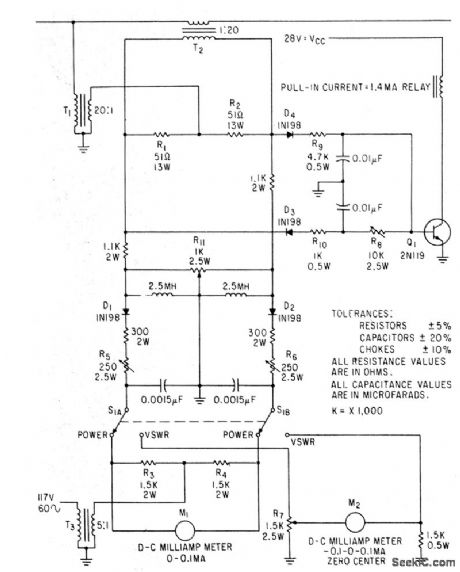
Standing-wave ratio is indicated by position of shaft of potentiometer R7 in bridge circuit, when switch is in vswr position. Diodes D3 and D4 act with Q1 as alarm circuit that interrupts power amplifier plate voltage when vswr exceeds preset limit. At other switch position, actual r-f output power in watts is indicated on d-c milliammeter.-L. F. Stein, Versatile R.F Monitor Shows Power and VSWR, Electronics, 36:13, p 44-46. (View)
View full Circuit Diagram | Comments | Reading(944)
COATING_THICKNESS_GAGE
Published:2009/7/17 2:23:00 Author:Jessie
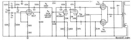
Oscillator V1 and amplifier V2-V3-V4 apply 10-cps signal to magnetic-reluctance transducer held over coating up to 0.040 inch thick, unbalancing transducer and giving output voltage proportional to thickness of coating. (View)
View full Circuit Diagram | Comments | Reading(766)
DIAMOND_CIRCUIT_MEASURES_A_F_PHASE_SHIFT
Published:2009/7/17 2:22:00 Author:Jessie
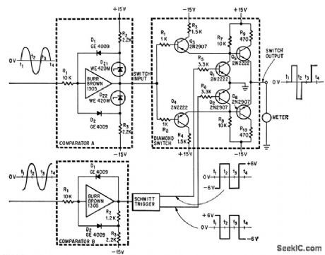
Accuracy is 1%UP to 2,000 cps. Used in computers and for high-speed analog instrumentation. Zero-center d-c ammeter indicates negative value for zero phase shift, zero for 90° phase shift,and some maximum value for 180° phase shift.-H. R. Deveraux, Diamond Circuit Measures Phase Shill,Electronics,37:25,p 74-75. (View)
View full Circuit Diagram | Comments | Reading(1126)
MEASURING_TRANSISTOR_OPEN_CIRCUIT_OUTPUT_ADMITTANCE
Published:2009/7/17 2:20:00 Author:Jessie
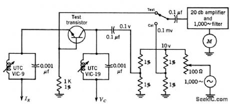
Test set gives smallsignal value h-ob of open-circuit output admittance of transistor for common-base connection. Input voltage is held constant at 1 V and current is read as voltage drop across 1K resistor. Voltage in mv can then be read directly as admittance of 0.1 to1 micromho on 10-mv scale of meter.-Texas Instruments Inc., Transistor Circuit Design, McGraw-Hill, N.Y., 1963, p 71. (View)
View full Circuit Diagram | Comments | Reading(1114)
MAGNETIC_TAPE_FLUTTER
Published:2009/7/17 2:19:00 Author:Jessie
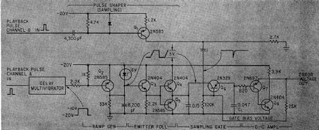
Time of travel of recorded pulse between two playback heads on lope recorder under lest is converted to d-c voltage. Boxcar detection circuit, ramp generator, and sampling gate detect flutter components as small as 0.01 % peak-topeak.-A. Schulback, Instantaneous Measurement of Tape Flutter, Electronics, 35:19, p 93-94. (View)
View full Circuit Diagram | Comments | Reading(869)
4013_DIVIDE_BY_2_CIRCUT
Published:2009/7/17 2:11:00 Author:Jessie
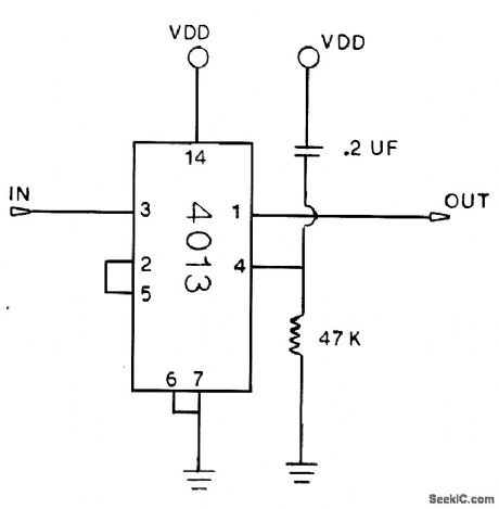
The first pulse into the input drives the output high. The second pulse drives the output low. VCC can be 5 to 15 V. (View)
View full Circuit Diagram | Comments | Reading(2151)
MEASURING_CONVERSION_GAIN
Published:2009/7/17 2:05:00 Author:Jessie
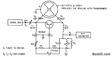
Used form measuring input impedance characteristics of high-frequency transistor for operation beyond cutoff in special converter circuits.-V.W.Vodicka and R.Zuleeg, Transistor Operation Beyond cutoff Frequency, Electronics,33:35,p 56-60. (View)
View full Circuit Diagram | Comments | Reading(824)
NOISE_FIGURE_MEASUREMENT_OF_R_F_TUBES
Published:2009/7/17 2:04:00 Author:Jessie
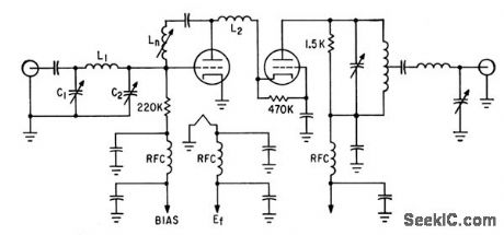
Standardized EIA Committee circuit measures noise-figure of cascode r-f amplifiers with 95% repeatability Jig circuit for ,tube under lest has 200-Mc center frequency and 10-Mc bandwidth,-T .E. Gausman, Standardizing Noise-Figure Measurement, Electronics,36:1,p 124-129. (View)
View full Circuit Diagram | Comments | Reading(885)
CAPACITANCE_TRACKING_TEST_SET
Published:2009/7/17 2:03:00 Author:Jessie
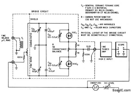
Output signal voltage of capacitance bridge, proportional to capacitance unbalance, is applied to vertical input of scope through 1-Mc preamp. Horizontal sweep voltage of scope is also applied as bias to voltage-variable capacitances VVC whose tracking is being measured, so scope display shows diode capacitance-tracking as function of bias voltage.-L. A. Weldon and R. L. Kopski, Boost for Electronic Tuning, Electronics, 37:14,p 61-63. (View)
View full Circuit Diagram | Comments | Reading(1189)
28_MHz_TO_220_MHz_FOR_TRANSMIT
Published:2009/7/11 5:16:00 Author:May
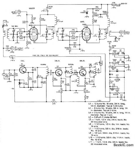
Permits use of 2-meter transceiver to transmit in 220-MHz band with minimum of 6-W power output for 1-W drive on 28 MHz Local-oscillator output at 192 MHz can be used for receiving converter as well Use 8-pF butterfly-type air variable(Johnson 160-028-001)for C24, C26, C28, and C32,D1 is GE ZD8. 28-V1-Wzener,-F. J. Merry、A220-MHz Transmit Converter, QST, Jan, 1978, p 16-20. (View)
View full Circuit Diagram | Comments | Reading(1346)
MOSSBAUER_EFFECT_SPECTROMEIER
Published:2009/7/17 2:01:00 Author:Jessie
Circuit makes effective use of transistors as current amplifiers.-W. W. MacDonald, Electronics in Israel, Electronics, 37:3, p 23-29. (View)
View full Circuit Diagram | Comments | Reading(905)
TRANSISTOR_TESTER_1
Published:2009/7/11 5:14:00 Author:May
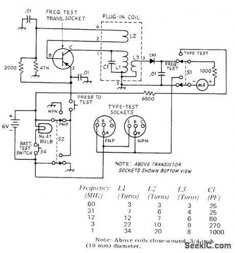
Determlnes maxlmum frequency at which unknown transistor will still maintain reasonable current gain, and tells whethertransistor is NPN or PNP. Based on fact that emitter-base junction of transistor is equivalent to crystal diode, conducting in one direction only. Direction depends on transistor type. Setting of S2 which gives meter reading identifies transistor type. Frequency-limit circuit is self-excited oscillator in which frequency de. pends on plug-in coil. If meter reads when 60MHz coil is used, transistor is capable of handling 60 MHz; if no reading, change to lower-frequency coils one by one until reading is obtained. To check battery, press S4; lamp should have full brilliance. CR1 is 1N34A.-H. Hanson, How High Will It Go?, QST, April 1974, p 32-33 and 39. (View)
View full Circuit Diagram | Comments | Reading(1308)
MAGNETIC_TAPE_SKEW_MEASUREMENT
Published:2009/7/17 1:58:00 Author:Jessie
Magnetic strip recorded on tape is scanned transversely with ring-type play-back head, and periods between output pulses generated at crossover points are measured. C1 acquires positive charge for one direction of skew and negative charge for other. Output of detector of C1, which measures this charge, is fed to difference amplifier having microammeter connected between cathodes to read tracking error.-B. R. Gooch, Magnetic Strip Keeps Tape Running True,Electronics,36:2, p42-43. (View)
View full Circuit Diagram | Comments | Reading(785)
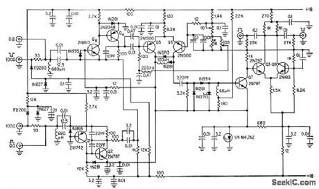
PB_SWITCH_ACTIVATED_MEMORY
Published:2009/7/17 1:55:00 Author:Jessie
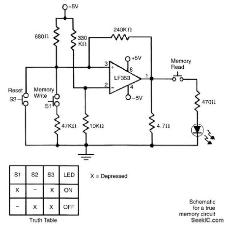
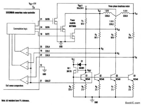
Many new brushless-motor control schemes use ICs that determine the rotor position by sensing the motor's back-BMP signals. In a unipolar configuration, the control chip synchronizes the three phases of drive currents by detecting the moments when each back-EMF signal rises just above, or falls just below, the motor supply voltage, VBATT (see the figure), These instances are known as zero crossings. This circuit shifts the signals down to a reference level, VREF The MOSFET, M1, along with resistor R1 and NPN transistor Q1, creates a reference current (I1) that is equal to (VBATT-VREF)/R1.This reference current is replicated in Q2, Q3, and Q4. Because R2=R3=R4=R1, the voltage drop across each resistor is the same. That means that V2,V3and V4 vary above and below VBATT the same amount as V2,V3,and V4 vary above and below VBATT Matching resistors R1 to R4 within 1 percent and matching R5 to R8 within 1 percent will resolve back-EMF signals as small as 200 mV. Diode D1 protects M1's gate from large transients on VBATT. The ESD diodes on the 551595, along with resistors R2, R3, and R4, protect the IC from damaging transients at V2,V3 and V4. (View)
View full Circuit Diagram | Comments | Reading(1954)
LOGIC_PROBE_1
Published:2009/7/17 1:48:00 Author:Jessie
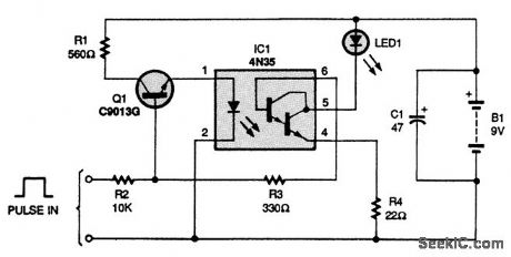
The circuit uses a 4N35 optocoupler (IC1) and a C9013G transistor (Q1). A positive pulse at the base of Q1 turns on the transistor. The 10,000-Ω resistor (R2) limits the incoming pulse so as not to feed too much current to the base of Q1, preventing the transistor from being damaged. With the base of Q1 at a positive potential, electron current flows from the emitter to the collector junction. The incoming pulse also pulls pin 6 high, lighting up LED1 by allowing current to flow between pins 4 and 5. The 330-Ω resistor (R3) provides current limiting for pin 6, although R4 is the current limiter for pin 4. While testing a digital circuit, if the LED lights, that portion of the circuit is in a high state; if the LED remains off, a low is present. The circuit can be placed inside a small enclosure if its connections are made as short as possible. (View)
View full Circuit Diagram | Comments | Reading(6687)
OPAMP_TESTER
Published:2009/7/11 5:12:00 Author:May
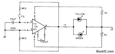
Developed for quick testing of 741 and 301 opamps. For good opamp, LEDs flash alternately with 1-s period. No flashing and no illumination indicate opamp output fault. If one of LEDs glows continuously, one of inputs is faulty. Asymmetrical blinking indicates leakage in opamp.-Circuits, 73 Maga-zine, March 1977, p 152. (View)
View full Circuit Diagram | Comments | Reading(2824)
PULSE_COINCIDENCE_DETECTOR
Published:2009/7/11 4:59:00 Author:May
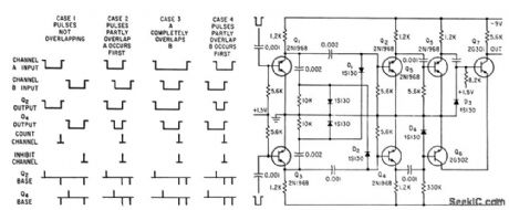
Detecls coincidences between pulses of random length and spacing occurring in two separctte channels, to permit counting only pulses that do not overlap.-K. R. Whittington and G. Robson, Novel Anticoincidence Circuit Detects Pulse overlap, Electronics, 35:26, p82. (View)
View full Circuit Diagram | Comments | Reading(0)
QUAD_OPAMP_TESTER
Published:2009/7/11 4:39:00 Author:May
Interface circuit shown permits use of single-opamp tester for testing quads without major modification of tester's original function. Interface operates on power available from tester, which can be Teledyne/Philbrick 5102 or current Tektronix or ESI testers. CM0S input transmission gates IC1 and IC2, supply input signals to sections of device under test (DUT). Gate control signals are supplied by section selector S1; switch can be automated by using two-line BCD selection, Same switch also activates reed relay that cona nects respective amplifier section to load and output monitoring circuits of tester. LEDs indicate section under test. Interface can be used with LM124, CA124, and MC3503 series of quad opamps.-A. C. Svoboda, Use a Single Op-Amp TesterforQuads, EDN Magazine, March 5, 1975, p76. (View)
View full Circuit Diagram | Comments | Reading(1569)
WEAK_SIGNAL_DECODER
Published:2009/7/11 4:35:00 Author:May
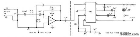
Combination of narrow-bandpass 800-Hz active filter and phase-locked loop of tone decoder permits copying very weak signals in Morse code. LED provides visual indication supplementing conventional output for headphones or loudspeaker.-Circuits, 73 Magazine, July 1977, p 35. (View)
View full Circuit Diagram | Comments | Reading(818)
| Pages:41/101 At 204142434445464748495051525354555657585960Under 20 |
Circuit Categories
power supply circuit
Amplifier Circuit
Basic Circuit
LED and Light Circuit
Sensor Circuit
Signal Processing
Electrical Equipment Circuit
Control Circuit
Remote Control Circuit
A/D-D/A Converter Circuit
Audio Circuit
Measuring and Test Circuit
Communication Circuit
Computer-Related Circuit
555 Circuit
Automotive Circuit
Repairing Circuit