
Index 50
PEAK_PROGRAM_DETECTOR
Published:2009/7/9 23:22:00 Author:May
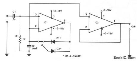
This circuit will allow a multimeter to display the positive or negative peaks of an incoming signal. A 741, IC1, is used in the noninverting mode with R1 defining the input impedance. D1 or D2 will conduct on a positive or negative peak, charging C2 until the inverting input is at the same dc level as the incoming peak. This level will maintain the voltage until a higher peak is detected, then this will be stored by C2. Another 741, IC2, prevents loading by the multimeter. Connected in the noninverting mode as a unity gain buffer, output impedance is less than 1 Ω. This circuit has a useful frequency response from 10 Hz to 100 kHz at ± 1 dB. High linearity is ensured by placing the diodes in the feedback loop of IC1, effectively compensating for the 0.6 V bias that these components require. (View)
View full Circuit Diagram | Comments | Reading(891)
STALLED_OUTPUT_DETECTOR
Published:2009/7/9 23:22:00 Author:May
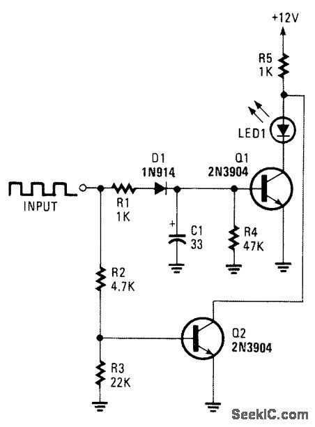
This circuit can be used to detect a stuck out-put or node in a circuit, or a loss of data or pulses.The pulse train charges C1 and biases Q1 on, which lights the LED. If the input remains high, Q2 extin-guishes the LED. (View)
View full Circuit Diagram | Comments | Reading(797)
AUDIO_MILLIVOLTMETER_1
Published:2009/7/9 23:02:00 Author:May
This circuit has a flat response from 8 Hz to 50 kHz at -3 db on the 10-mV range. The upper limit remains the same on the less sensitive ranges, but the lower frequency limit covers under 1 Hz. (View)
View full Circuit Diagram | Comments | Reading(1058)
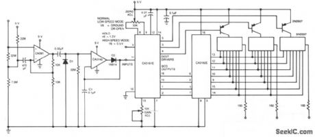
HALF_STEP_DRIVE_STEPPER_MOTOR
Published:2009/7/9 23:01:00 Author:May
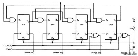
Clock pulses are converted to the switching sequence necessary for a four-phase stepper through 400 half steps of 0.9°each. (View)
View full Circuit Diagram | Comments | Reading(1558)
FREQUENCY_COUNTER
Published:2009/7/9 22:59:00 Author:May
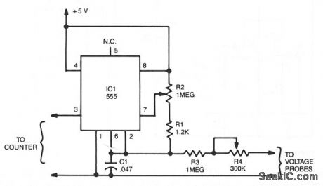
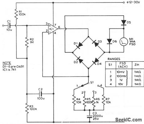
The output frequency from IC pin 3 is determined by the voltage input to pin 6. A standard frequency counter can be used to measure voltages directly over a limited range from 0 to 5 V. In this circuit, the 555 is wired as an astable multi ibrator. Resistor R2 determines the output frequency when the input to the circuit (the voltage measured by the voltage probes) is zero. R4 is a scaling resistor that adjusts the output frequency so that a change in the input voltage of 1 V will result in a change in the output frequency of 10 Hz. That will happen when the combined resistance of R3 and R4 is 1.2 MΩ. To calibrate short the voltage probes together, adjust R2 until the reading on the frequency counter changes to 00 Hz. Then, use the voltage probes to measure an accurate 5-V source and adjust R4 until the frequency counter reads 50 Hz. (View)
View full Circuit Diagram | Comments | Reading(2814)
HIGH_NPUT_RESISTANCE_VOLTMETER
Published:2009/7/9 22:51:00 Author:May
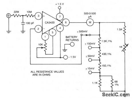
A resistance of 1,000,000 MΩ takes advantage of the high input impedance of the CA3420 BiMOS op amp. Only two 1.5-V AA-type penlite batteries are required for use. Full-scale deflection is ±1500 mV. ±150 mV and ±15 mV. (View)
View full Circuit Diagram | Comments | Reading(841)
AUDIO_MILLIVOLTMETER
Published:2009/7/9 22:47:00 Author:May
Capacitor C4 couples the output of U1 to a simple attenuator, which is used to provide a loss of 0 dB, 20 dB, or 40 dB, depending on the setting of range switch S1. The circuits sensitivity is 10-V rms for fullscale deflection, so the attenuator gives additional ranges of 100-mV and 1-V rms. The attenuator output is connected through capacitor C5 to common-emitter amplifier Q1, which has a high-voltage gain of 40 dB.To get linear scaling on the meter, we have to use an active-rectifier circuit built around U2. That IC is connected so that its noninverting input is biased to the 0-V bus via R7. Capacitor C6 couples the output of Q1 to the noninverting input of U2; C7 is the compensation capacitor for U2.The voltage gain of U2 is set by the difference in resistance between the output and the inverting input, and between the inverting input and the ground bus. One resistance is made up of the diode-bridge rectifier D1 through D4, the other by resistor R8. This circuit has a nearly flat frequency response to about 200 kHz. (View)
View full Circuit Diagram | Comments | Reading(1503)
CONTINUITY_TESTER
Published:2009/7/9 22:43:00 Author:May
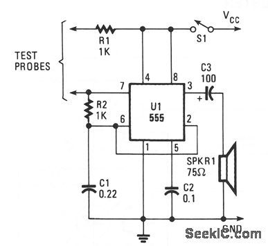
The continuity tester feeds a voltage throughthe positive probe to the circuit-under-test, whilethe negative probe serves as the return line. Voltage that rettion to the tester through the negative probe triggers circuit, giving an audible indication of continuity. (View)
View full Circuit Diagram | Comments | Reading(4733)
VOLTAGE_MONITOR
Published:2009/7/9 22:42:00 Author:May
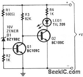
If the battery voltage exceeds about 11 V, current flows through R1, D1, and R2. The voltage produced as a result of current flow through R2 is sufficient to bias transistor Q1 into conduction. That places the collector voltage of Q1 virtually at ground. Therefore, Q2, driven fromthe collector of Q1, is cut off, LED1 and current-limiting resistor R4 are connected in the collector circuit of Q2. With Q2 in the cut-off state, the LED does not light. Should Q1's base voltage drop below approxi-mately 0.6 V. Q1 turns off. biasing Q2 on and illuminating LED1 to indicate that the battery voltage has fallen below the 11 V threshold level. (View)
View full Circuit Diagram | Comments | Reading(0)
CABLE_TESTER
Published:2009/7/9 22:40:00 Author:May
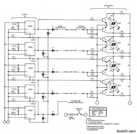
This compact tester checks cables for open-circuit or short-circuit conditions. A differential transistorpar at one end of each cable line remalns balanced as long as the same clock pulse generated bjy timer IC appears at both ends ofthe line. A clock pulse,just at the clock end of the line, lights a green LED,and aclock pulse,only at the other end,lights a red LED. (View)
View full Circuit Diagram | Comments | Reading(0)
DIODELESS_PRECISION_RECTIFIER
Published:2009/7/9 22:38:00 Author:May

A CA3130 BiMOS op amp, acts as an attenuator for positive inputs and as a conventional op amp fornegative signals. With 1-V rms input and a circuit gam of 0.8, its frequency response is -1%at 60 kHz and-1 dB at 300 kHz. (View)
View full Circuit Diagram | Comments | Reading(955)
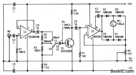
SENSITIVE_RF_VOLTMETER
Published:2009/7/9 22:37:00 Author:May
This schematic shows a peak-reading diode voltmeter driven by two stages of amplification. A 100-μF capacitor provides a fairly large time constant, which results in satisfactory meter damping. The limited differential output voltage coupled with an overdamped meter prevents most needle pinning when you select an incorrect range position, or make other errors. An SPST toggle switch selects additional series resistance. This X2 function gives some more overlap of the sensitivity ranges. The resistance values shown are correct for use with a 100-μA meter with 1500-Ω internal resistance. (View)
View full Circuit Diagram | Comments | Reading(1562)
INTEGRATED_AM_RECEIVER
Published:2009/7/9 22:33:00 Author:May

This circuit has aerial and local oscillator circuits for a 27-MHz recelver for remote control of garagedoors, projectors, curtains, etc. (View)
View full Circuit Diagram | Comments | Reading(1212)
FET_VOLTMETER
Published:2009/7/9 22:31:00 Author:May
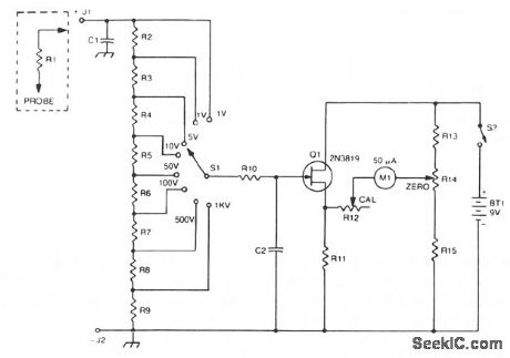
A2N3819 FET provides a solid-state VOM。The 2N3819 acts as a cathodefollowerin a VOM.The biasoffset(meter null) is obtained with R14 and R12 sets full-scale calibration R2 through R9 should totalabout10 MΩ.R10 is a protective resistor, and C2 provides ac bypassing to limit rf and noise pickup, (View)
View full Circuit Diagram | Comments | Reading(0)
ACOUSTIC_DOPPLER_MOTION_DETECTOR
Published:2009/7/9 22:25:00 Author:May
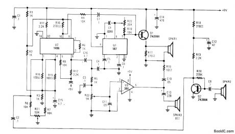
A high-frequency audio signal (15 to 25 kHz) generated by U1 is fed to buffer Q1 and SPKR1. A por-tion is fed to balanced mixer U2. Received audio picked up by SPKR2 (used as a microphone) is amplifted by Q2 and fed to U2. When sound is reflected from a moving object, the Doppler effect will cause an apparent shift in frequency. U2 produces a signal equal to the frequency difference. This is coupled via C16 and gain control R23 to amplifier U3, where the beat note is heard in SPKR3. (View)
View full Circuit Diagram | Comments | Reading(1089)
AC_VOLTMETER
Published:2009/7/9 22:25:00 Author:May
CA081 and CA3140 BiMOS op amp offer minimal loading on the circuits being measured。The wide bandwidth and high slew rate of the CA081 allow the meter to operate up to 0.5 MHz, (View)
View full Circuit Diagram | Comments | Reading(2046)
UHF_MOTION_DETECTOR
Published:2009/7/9 22:16:00 Author:May


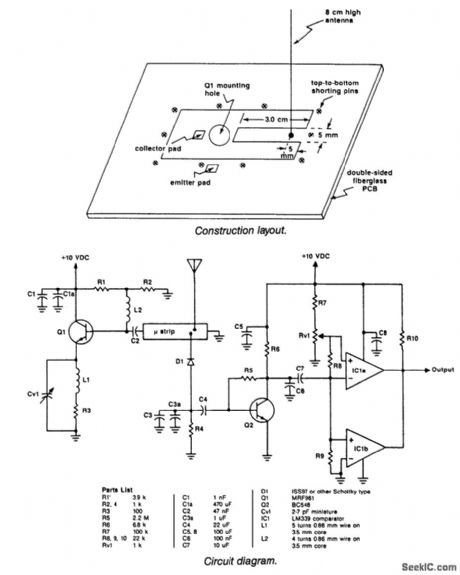
The UHF motion detector operates on the Doppler radar principle. Q1 is an oscillator that creates a adiated signal. An object in the radiated field reflects some of this energy back to the detector. If the ect is moving, the reflected signal will have a different frequency because of Doppler shift.Q1 is an oscillator coupled to a small (8-cm) antenna. This antenna also receives the reflected signal. D1 acts as a mixer and produces a beat note of frequency that is equal to the difference in reflected nd radiated signal. Q2 amplifies this signal and couples it to comparator/detector IC1A and IC1B. The utput can continue on to an alarm, relay, lamp,etc. (View)
View full Circuit Diagram | Comments | Reading(3851)
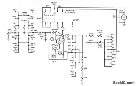
DC_VOLTIETER
Published:2009/7/9 22:14:00 Author:May
This dc voltmeter, with high input resistance, uses a CA3130 BiMOS op amp and measures voltages from 10 mV to 300 V. Resistors R12 and R14 are used individually to calibrate the meter for full-scale deflection. Potentiometer R6 is used to null the op amp and meter on the 10-mV range by shorting the input terminals, then adjusting R6 for the first indication of upscale meter deflection. (View)
View full Circuit Diagram | Comments | Reading(1564)
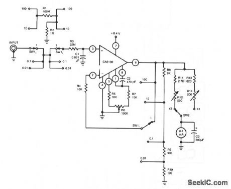
HIGH_INPUT_RESISTANCE_DC_VOLTMETER
Published:2009/7/9 22:12:00 Author:May
This voltmeter exploits a number of the CA3160 BiMOS op amp's useful characteristics. The available voltage ranges from 10 mV to 300 V. Powered by a single 8.4-V mercury battery, this circuit, with zero input, consumes approximately 500 μA. Thus, at full-scale input, the total supply current will increase by 1000 μA. (View)
View full Circuit Diagram | Comments | Reading(992)
OVER_UNDER_VOLTAGE_MONITOR
Published:2009/7/9 22:09:00 Author:May

Any potential from 1 to 15 V can be monitored with this circuit. Two lamps alert any undesirable variation. The voltage differential from lamp turn-on to turn-off is about 0.2 V at any setting. High and low set points are independent of each other. The SCRs used in the circuit should be the sensitive gate type. R3 must be experimentally determined for the particular series of SCRs used. This is done by adjusting R3 to the point where the undervoltage lamp turns on when no signal is present at the SCR2 gate. Any 15-V segment can be monitored by putting the zener diode. D1. in series with the positive input lead. The low set-point voltage will then be the zener voltage plus 0.8 V. (View)
View full Circuit Diagram | Comments | Reading(928)
| Pages:50/101 At 204142434445464748495051525354555657585960Under 20 |
Circuit Categories
power supply circuit
Amplifier Circuit
Basic Circuit
LED and Light Circuit
Sensor Circuit
Signal Processing
Electrical Equipment Circuit
Control Circuit
Remote Control Circuit
A/D-D/A Converter Circuit
Audio Circuit
Measuring and Test Circuit
Communication Circuit
Computer-Related Circuit
555 Circuit
Automotive Circuit
Repairing Circuit