
Signal Processing
Index 15
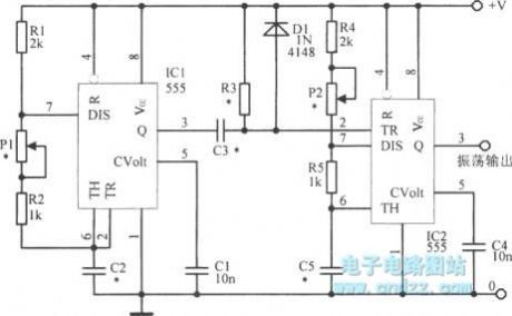
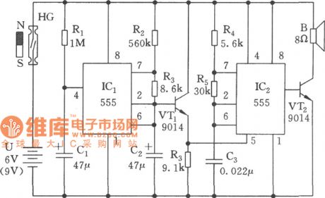
Tape recorder clock oscillator
Published:2013/2/21 0:47:00 Author:Ecco | Keyword: Tape recorder , clock oscillator
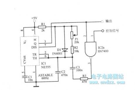
Tape recorder clock oscillator is shown as figure.
(View)
View full Circuit Diagram | Comments | Reading(931)
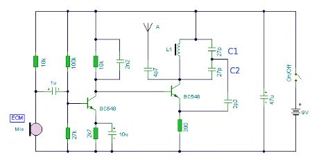
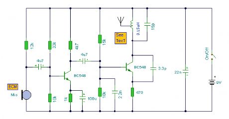
2 Transistor FM Transmitters
Published:2013/2/19 20:37:00 Author:muriel | Keyword: 2 Transistor , FM Transmitters
View full Circuit Diagram | Comments | Reading(986)
0 ~ +30 mV unipolar input , 4 ~ 20mA output circuit with multi-functional sensor signal conditioner AD693
Published:2013/2/19 1:26:00 Author:Ecco | Keyword: 0 ~ +30 mV , unipolar input, 4 ~ 20mA, output , multi-functional sensor , signal conditioner
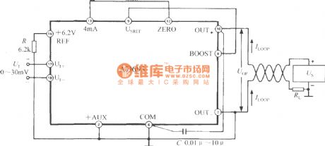
The loop power Us allowable range is +12 ~ +36 V. RL is a load resistor in the current loop, iLoop is the loop current.
(View)
View full Circuit Diagram | Comments | Reading(1295)
The broadband pulse generator with independently adjustable duty cycle
Published:2013/2/19 2:25:00 Author:Ecco | Keyword: broadband pulse generator , independently , adjustable, duty cycle
The broadband pulse generator with independently adjustable duty cycle is shown as figure.
(View)
View full Circuit Diagram | Comments | Reading(1145)
Pulse oscillator with adjustable duty cycle and frequency
Published:2013/2/18 2:11:00 Author:Ecco | Keyword: Pulse oscillator, adjustable duty cycle , frequency
Pulse oscillator with adjustable duty cycle and frequency is shown as figure.
(View)
View full Circuit Diagram | Comments | Reading(1549)
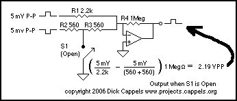
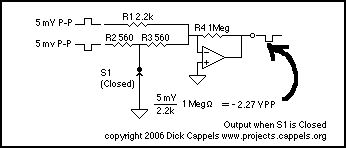
Signal acquisition and processing circuit diagram
Published:2013/2/18 0:10:00 Author:Ecco | Keyword: Signal acquisition , processing
Signal acquisition and processing circuit diagram is shown as figure.
(View)
View full Circuit Diagram | Comments | Reading(1155)
FM Transmitter 1
Published:2013/2/17 20:29:00 Author:muriel | Keyword: FM Transmitter
View full Circuit Diagram | Comments | Reading(945)
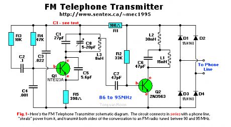
Telephone Transmitter
Published:2013/2/17 20:27:00 Author:muriel | Keyword: Telephone Transmitter
View full Circuit Diagram | Comments | Reading(1152)
Variable pitch multivibrator circuit diagram
Published:2013/1/31 0:44:00 Author:Ecco | Keyword: Variable pitch, multivibrator
This circuit is composed of two 555 time-base circuits, and it can issue 400 ~ 2500Hz oscillatory wave with continuous changes, it is similar to the sound of public security police vehicles. The circuit consists of the boot delay, low-frequency oscillator and modulated tone generator.
(View)
View full Circuit Diagram | Comments | Reading(1319)
High-stability Wien bridge oscillator circuit
Published:2013/1/30 1:46:00 Author:Ecco | Keyword: High-stability , Wien bridge , oscillator

View full Circuit Diagram | Comments | Reading(1241)
Asymmetric square wave circuit
Published:2013/1/30 1:48:00 Author:Ecco | Keyword: Asymmetric square wave
Asymmetric square wave circuit is shown as figure.
(View)
View full Circuit Diagram | Comments | Reading(1644)
Keying freedom multivibrator circuit
Published:2013/1/30 1:47:00 Author:Ecco | Keyword: Keying freedom multivibrator

Keying freedom multivibrator circuit is shown as figure.
(View)
View full Circuit Diagram | Comments | Reading(909)
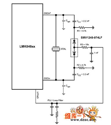
LMK04000 reference design schematics with crystal oscillator
Published:2013/1/29 2:26:00 Author:Ecco | Keyword: reference design , crystal oscillator
View full Circuit Diagram | Comments | Reading(898)
The music scale signal generator (NE555, CD4017)
Published:2013/1/29 2:25:00 Author:Ecco | Keyword: music scale, signal generator
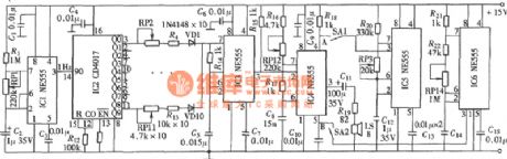
The musical scale signal is a kind of oscillation pulse which is arranged a certain frequency interval, it can be generated by mechanical vibration of the various instruments, and also can be generated by oscillator composed of the electronic circuit. The oscillator with digital circuit can generate l0 octaves Loops by stepping control, and the circuit is shown in the figure. The circuit consists of basic scale oscillator, stepper pulse oscillator and scale interval control circuit and other components.
(View)
View full Circuit Diagram | Comments | Reading(1501)
Harmonic generator (LM318)
Published:2013/1/28 2:03:00 Author:Ecco | Keyword: Harmonic generator
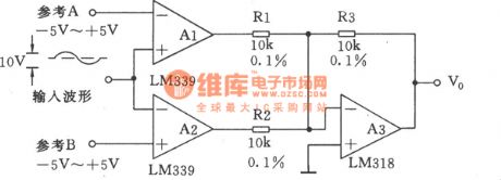
The harmonics generator composed of two comparators and a summing amplifier is shown in Figure. It can make use of any non- party sine, triangle, sawtooth waveform to get the harmonic which can be widely used in phase-locked loop, waveform generator, electronic musical instruments and other harmonic applications.
(View)
View full Circuit Diagram | Comments | Reading(1858)
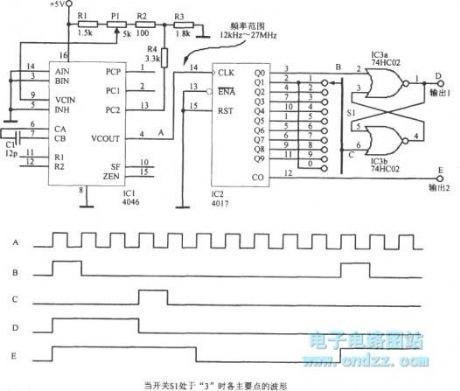
Frequency shift keying (FSK) square wave generator with CD4046B
Published:2013/1/28 2:11:00 Author:Ecco | Keyword: Frequency shift , keying, FSK, square wave generator
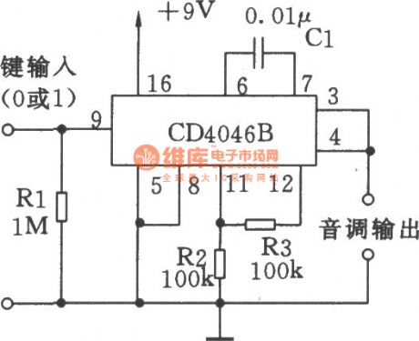
The keying signal is applied to control input end-pin 9 of CD4046, when the keying input is 1 level, the circuit will generate 2.4kHz audio frequency; when the input is 0 level, it will generate l.2kHz audio frequency. High - frequency tones are preset by the component values of Cl and Rl, and low-frequency tones is preset by the value of Cl, R2 and R3.
(View)
View full Circuit Diagram | Comments | Reading(3091)
Oblique wave generator with CD4046
Published:2013/1/28 2:14:00 Author:Ecco | Keyword: Oblique wave generator
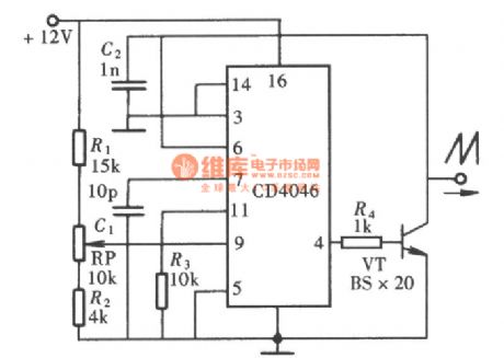
The external capacitor connected to CD4046's pin ⑥, ⑦ is divided into two parts, namely grounded. Because their charge and discharge time is different, the waveform generated by voltage-controlled oscillator can have a huge difference in the rising and falling edges.
(View)
View full Circuit Diagram | Comments | Reading(2709)
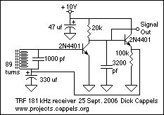
simple TRF receiver
Published:2013/1/22 21:21:00 Author:muriel | Keyword: simple, TRF receiver
View full Circuit Diagram | Comments | Reading(0)
Switched resistor modulator 2
Published:2013/1/22 21:19:00 Author:muriel | Keyword: Switched, resistor modulator
View full Circuit Diagram | Comments | Reading(835)
Switched resistor modulator
Published:2013/1/22 21:18:00 Author:muriel | Keyword: Switched , resistor modulator
View full Circuit Diagram | Comments | Reading(851)
| Pages:15/195 1234567891011121314151617181920Under 20 |
Circuit Categories
power supply circuit
Amplifier Circuit
Basic Circuit
LED and Light Circuit
Sensor Circuit
Signal Processing
Electrical Equipment Circuit
Control Circuit
Remote Control Circuit
A/D-D/A Converter Circuit
Audio Circuit
Measuring and Test Circuit
Communication Circuit
Computer-Related Circuit
555 Circuit
Automotive Circuit
Repairing Circuit