
Basic Circuit
Index 337
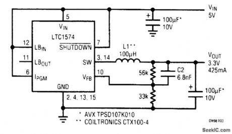
5_TO_33_V_SURFACE_MOUNT_SWITCHING_REGULATOR
Published:2009/6/24 5:29:00 Author:May
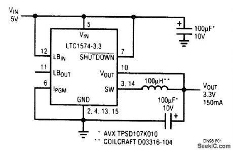
This converter provides 3.3 V at 150 mA from an input voltage of 5 V. Peak inductor current is limited to 340 mA by connecting pin 6 (IPGM) to ground. For applications requiring higher output current, connect pin 6 to Vin. Under this condition, the maximum load current is increased to 425 mA. (View)
View full Circuit Diagram | Comments | Reading(702)
POSITIVE_REGULATOR_SINKS_CURRENT
Published:2009/6/24 5:28:00 Author:May
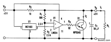
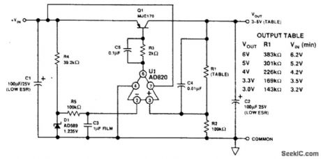
Generally speaking, conventional positive voltage regulators can only source current; they can't sink it. However, the positive regulator shown breaks that rule because it can perform both functions.The idea is to have the control transistor Q1 in shunt so that the regulator can either source or sink current.The circuit provides +3-V output from a +5-V supply. U1 is a bandgap reference that supplies a stable +2.5-V reference to the error amplifier (A1). The output voltage (VO) is sampled by the resis-tor network (R1 and R2). If VO were to increase, A1 will drive the base of Q1 harder, increasing the collector current (IC).This increases the drop across R3 and VO decreases, thus regulating the output voltage. The output voltage is givenby VO = 2.5(1 + R1/R2)Under no load conditions, Q1 draws 110 mA [(Vin-VO)/R3]. With a load connected, and as the regulator begins to source load current (IL), IC decreases to keep the drop across R3 constant.At IL 100 mA, Q1 carries 10 mA. If RL is connected to the positive supply higher than VO, then the regulator must sink current, and IL becomes negative. At IL = -100 mA, Q1 carries 210 mA while maintaining the output voltage at +3 V. The output voltage will remain constant at +3 V—even if the load current changes sign.With the proper heatsink on Q1, the regulator can sink more than 300 mA. If a sink only option is desired, the dissipation in Q1 can be reduced by using a 180-Ω resistor for R3. R4 limits the base current drive for Q1 and prevents the output of A1 from being clamped at 2 VBE. (View)
View full Circuit Diagram | Comments | Reading(1069)
SIMPLE_NOISE_LIMITER
Published:2009/6/24 5:25:00 Author:May
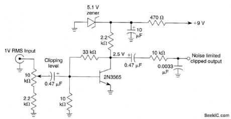
This circuit uses a symmetrical limiter obtained by biasing a transistor to a Q point that is half of the supply voltage and driving it into saturation and cutoff. An input of 1 to 2 V RMS is sufficient. This output will be approximately 4Vp-p into a high-impedance load. (View)
View full Circuit Diagram | Comments | Reading(1124)
ADJUSTABLE_NOISE_CLIPPER
Published:2009/6/24 5:22:00 Author:May
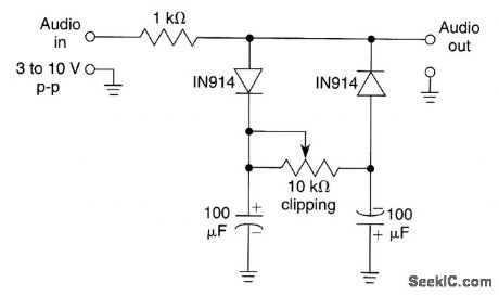
This circuit uses two diodes and is a peak-to-peak limiter. The capacitors charge up to a dc level determined by the peak-to-peak audio signal and the clipping control. A positive or negative peak or spike is clipped if it exceeds this level plus the diode drops. The circuit should be operated at several volts level for best results. (View)
View full Circuit Diagram | Comments | Reading(4208)
LOW_DROPOUT_REGULATOR
Published:2009/6/24 5:22:00 Author:May
This low-dropout reference produces a 4.5-V output from a supply just a few hundred mV loading, With 1-mA dc loading,it maintains a stable 4.5-V output for inputs down to 4.7 V. (View)
View full Circuit Diagram | Comments | Reading(0)
AUDIO_NOISE_BASED_VOTING_CIRCUIT
Published:2009/6/24 5:21:00 Author:May
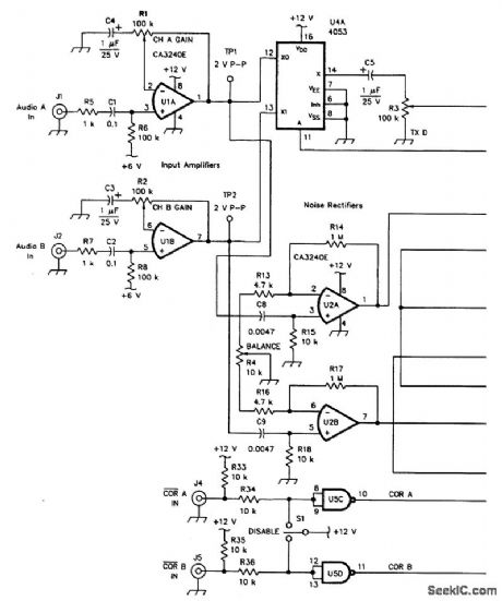
The purpose of this circuit is the selection of the output of two receivers, tuned to the same channel, that has the better signal to noise ratio. This circuit compares the two noise leads from the receivers and selects the one with the lower audio noise level. (View)
View full Circuit Diagram | Comments | Reading(789)
LOW_NOISE_REGULATOR(5_TO_33_V)
Published:2009/6/24 5:16:00 Author:May
In some applications, it is important not to introduce any switching noise within the audio frequency range. To circumvent this problem, a feed-forward capacitor can be used to shift the noise spectrum up and out of the audio band with C2 being the feed-forward capacitor. The peak-to-peak output ripple is reduced to 30 mV over the entire load range. A toroidal surface mount inductor L1 is chosen for its excellent self-shielding properties. (View)
View full Circuit Diagram | Comments | Reading(590)
DUAL_OUTPUT_REGULATOR
Published:2009/6/24 5:14:00 Author:May
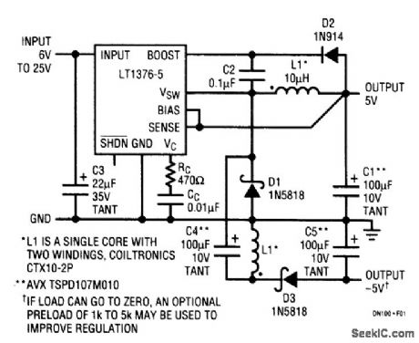
If load can go to zero, an optional preload of 1 to 5 kΩ can be used to improve regulation. Many modern circuit designs still need a dual polarity supply. Communication and data acquisition are typical areas where both 5 V and -5 V are needed for some of the IC chips.The current mode architecture and saturating switch design allow the LT1376 to deliver up to 1.5-A load current from the 8-pin SO package. L1 is a 10-μH surface-mount inductor from Coiltronics. The second winding is used to create a negative-output SEPIC (Single-Ended Primary Inductance Converter) topoLogy using D3, C4, C5, and the second half of F1. This converter takes advantage of the fact that the switching signal driving L1 as a positive buck converter is already the correct amplitude for driving a -5-V SEPIC converter. During switch-off time, the voltage across L is equal to the 5-V output plus the forward voltage of D1. An identical voltage is generated in the sec-ond winding, which is connected to generate -5 V using D3 and C5. Without C4, this would be a simple flyback winding connection with modest regulation. The addition of C4 creates the SEPIC topology. Note that the voltages swing at both ends of C4 is theoretically identical-even without the capacitor. The undotted end of both windings goes to a zero ac voltage node, so the equal windings will have equal voltages at the opposing ends. Unfortunately, coupling between windings is never perfect, and load regulation at the negative output suffers as a result. The addition of C4 forces the wind-ing potentials to be equal and (View)
View full Circuit Diagram | Comments | Reading(849)
DOLBΥ_NOISE_REDUCTION_CIRCUIT
Published:2009/6/24 5:14:00 Author:May
View full Circuit Diagram | Comments | Reading(718)
LOW_COST_STEP_DOWN_REGULATOR
Published:2009/6/24 5:10:00 Author:May
This inexpensive and efficient discrete step-down regulator is based on a complementary transistor arrangement that uses both positive and negative feedback and is referenced to a Zener diode. Inductor L1 is selected to maintain the switching frequency above the audible range for the intended operating load. The output filter L2 and C4 reduces ripple to less than 10 mV p-p over a large range of loads, with only a slight decrease in efficiency. (View)
View full Circuit Diagram | Comments | Reading(924)
33_V_1_A_SURFACE_MOUNT_REGULATOR
Published:2009/6/24 5:02:00 Author:May
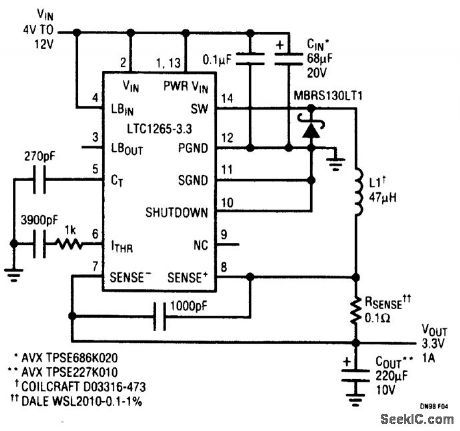
This figure shown a tuopical LTC1265 surface-mount application.It provides 3.3 V at 1 A from an input voltage range of 4 V to 12 V.The peak efficiency approaches 93% at mid-current levels. (View)
View full Circuit Diagram | Comments | Reading(692)
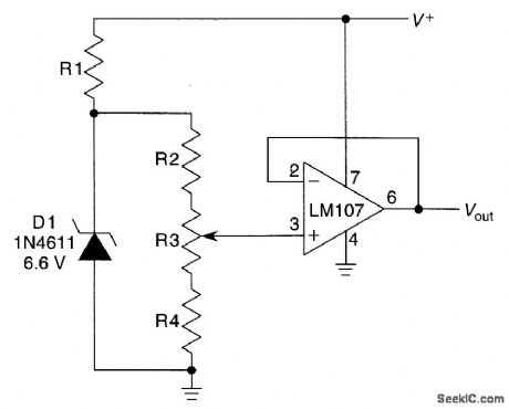
NEGATIVE_VOLTAGE_REFERENCE
Published:2009/6/24 5:01:00 Author:May
D1 is used as a reference. R2, R3, and R4 are voltage dividers to obtain desired output voltage to the op-amp voltage follower. (View)
View full Circuit Diagram | Comments | Reading(816)
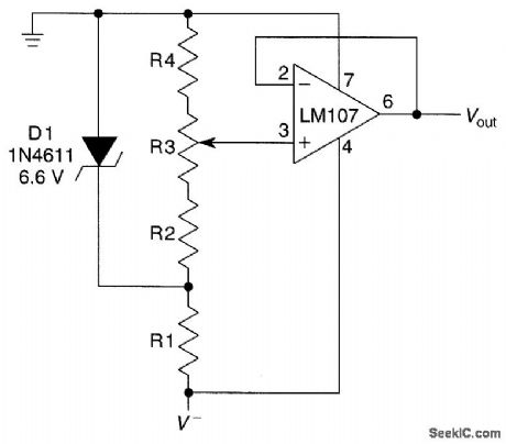
POSITIVE_VOLTAGE_REFERENCE
Published:2009/6/24 5:00:00 Author:May
D1 is used as a reference. R2, R3, and R4 provide desired output voltage to the op-amp voltage follower. (View)
View full Circuit Diagram | Comments | Reading(791)
LOW_VOLTAGE_REFERENCE
Published:2009/6/24 4:59:00 Author:May
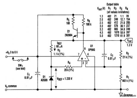
This circuit illustrates a number of techniques that are useful for low-voltage, series-mode, power-efficient references. Intended for output currents of up to 10 mA, this design has an enabled standby current of about 100 μA; it can be easily programmed over a wide range of output voltages. (View)
View full Circuit Diagram | Comments | Reading(777)
OLD_FASHIONED_CRYSTAL_RADIO
Published:2009/6/24 4:55:00 Author:May
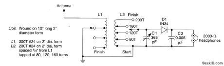
L1 and L2 are wound on 4 diameter 10 form and are 200 tums of #24 wire. PVC pipe can be used. (View)
View full Circuit Diagram | Comments | Reading(713)
VARIOMETER_TUNED_RADIO
Published:2009/6/24 4:54:00 Author:May


The two fixed coils of the variometer, L1 and L3, are wound on an S)G-inch-long piece of 1-inch-diameter plastic pipe (its outer diameter is about 1 1/4 inches). Each coil is 2 1/4 inches long. The num-ber of turns is not critical, but 86 tightly wound turns of #22 enameled wire were used. When winding the coils, make sure you start at a point that will allow them to be placed 2 inches apart on the pipe. Drill holes in the pipe and run the leads of the coils out the end of the pipe that is closest to each.The movable coil, L2, is wound on a piece of 1 1/2-inch plastic pipe (its outer diameter is about 1 7/8inches). The winding is 2 inches long. Like L1 and L3, the actual number ofwindings of this coil are not critical, as long as the winding is approximately the right length. (View)
View full Circuit Diagram | Comments | Reading(884)
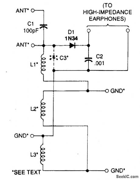
SUPERHET_FRONT_END
Published:2009/6/24 4:36:00 Author:May
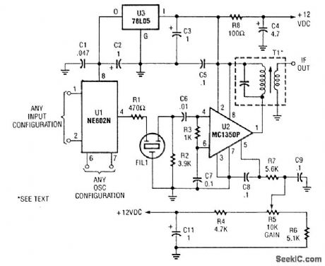
This superhet receiver front end is simple and uses an NE602 followed by an MC1350 IF amplifier. (View)
View full Circuit Diagram | Comments | Reading(0)
CAPACITOR_DISCHARGE_IGNITION_SYSTEM
Published:2009/6/24 4:22:00 Author:May
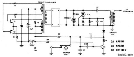
View full Circuit Diagram | Comments | Reading(0)
DIFFERENTIAL_THERMOMETER
Published:2009/6/24 4:18:00 Author:May
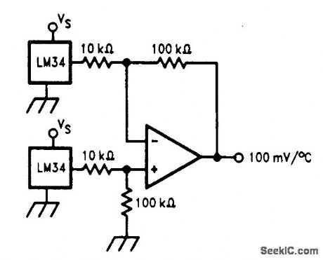
The differential thermometer shown in the figure produces an output voltage which is proportional to the temperature difference between two sensors. This is accomplished by using a dif-ference amplifier to subtract the sensor outputs from one another and then multiplying the differ-ence by a factor of 10 to provide a single-ended output of 100 mV per degree of differential tem-perature. (View)
View full Circuit Diagram | Comments | Reading(0)
ABSOLUTE_TEMPERATURE_LOG_WITH_RS_232
Published:2009/6/24 4:08:00 Author:May
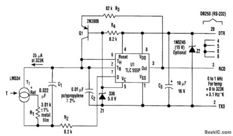
In the setup, T1 (an LM334 temperature sensor) generates a constant current that's propor-tional to absolute temperature, and equal to 25μA at 323 Kelvin (50℃). RI sets this constant of pro-portionality. The current discharges the parallel combination of C1 and C2 connected to the trigger and the threshold pins of UI, which is a CMOS implementation of the venerable 555 analog timer.The negative-going ramp is compared by UI to an internal2.S-V trigger level controlled by 21. When the ramp gets there, U1 triggers. The output pin (3) will go high, presenting a start bit to the con-nected communications port, which causes Q1 to source 100 μA to the timing node. At the same time, the discharge pin (7) will open, allowing R2 and the bottom end of C1 and T1 to be supplied by C1, and isolates it from C2.
Consequently, the current supplied by transistor Q1 will go solely to C2 so that when the result-ing positive-going ramp reaches 5V, exactly 25nC (2.5 V x C2) will have been deposited in the tim-ing node by the recharge cycle because its threshold level (6) will have been reached. This causes both the output pin to return to the negative rail, restoring the marking condition of the R2-232 in-terface, and Q1 to stop recharging C2. U1's discharge pin (7) now connects R2 to the negative rail, causing the charge that was deposited by T1 on C1 during the recharge interval to rapidly redistrib-ute between C1 and C2. This arrangement creates a very linear (0.01%) relationship between T1 cur-rent and pulse output frequency.
While this is happening, the PC's communications port hardware assembles a valid (although meaningless) character because the positive pulse output by UI looks like the start bit of a charac-ter. A simple program running in the PC can then count the frequency of these characters and con-vert the resulting rate into a direct readout of temperature. Because of the 3.1-Hz/degree slope of frequency versus temperature, a 30-second average suffices for 0.01°resolution. (View)
View full Circuit Diagram | Comments | Reading(0)
| Pages:337/471 At 20321322323324325326327328329330331332333334335336337338339340Under 20 |
Circuit Categories
power supply circuit
Amplifier Circuit
Basic Circuit
LED and Light Circuit
Sensor Circuit
Signal Processing
Electrical Equipment Circuit
Control Circuit
Remote Control Circuit
A/D-D/A Converter Circuit
Audio Circuit
Measuring and Test Circuit
Communication Circuit
Computer-Related Circuit
555 Circuit
Automotive Circuit
Repairing Circuit