
Basic Circuit
Index 320
DEBOUNCER
Published:2009/6/29 2:57:00 Author:May
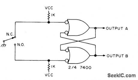
Generates single pulse on switch closure, provided wiper of switch bounces only between contact and an open. Output A goes low when switch is pushed, and at same time output B goes high.—E. E. Hrivnak, House Cleaning the Logical Way, 73 Magazine, Aug. 1974, p 85-90. (View)
View full Circuit Diagram | Comments | Reading(937)
12_W_OUTPUT
Published:2009/6/29 2:55:00 Author:May

Uses CA3094B programmable opamp to drive complementary- symmetry power-output transistors. Intermodulation distortion is only 0.2% when 60-Hz and 2-kHz signals are mixed in 4:1 ratio. Location of tone con| trols in feedback network improves signal-to-noise ratio. Hum and hoise are typically 700μV (83 dB down) at output. Transistor Q1 provides thermal compe"sation,-″Circuit Ideas for RCALinear ICs、″RCA Solid Stat Divsion、Somerville NJ、1977、p 11 (View)
View full Circuit Diagram | Comments | Reading(707)
Precision_absolute_value_circuit
Published:2009/7/24 22:17:00 Author:Jessie
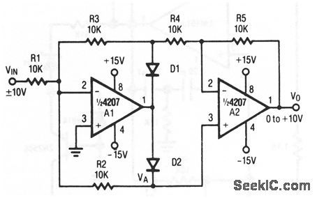
The values and types of D1 and D2 are not critical, but both diodes should be the same, and both must be able to withstand ±15 V (such as a 1N914). (View)
View full Circuit Diagram | Comments | Reading(1318)
BOUNCELESS_SQUARE_OUTPUT
Published:2009/6/29 2:39:00 Author:May
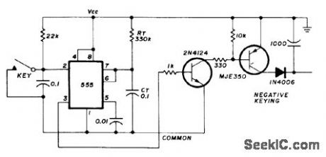
NE555 timer eliminates need for gates to suppress contact bounce. Timer can provide pulse at least 5 ms long (much longer if desired) and can remain on as long as trigger input (key pulse) is low (grounded). Timer triggers on negative-going edge of low-going pulse, such as key down to ground. Common negative is isolated from ground. VCC can be 5 to 15 VDC. Timer output can be connected directly to exciter keying input for negative grid keying. Because of square-wave output on make or break (100 ns each), circuits must be added in exciter or between keying transistors to provide at least 5-ms rise and fall times for Morse or RTTY key-ing.—B. Conklin, Improving Transmitter Keying, Ham Radio, June 1976, p 44-47. (View)
View full Circuit Diagram | Comments | Reading(648)
HIGH_GAIN_JFET
Published:2009/6/29 2:38:00 Author:May
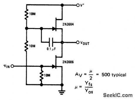
Simpletwo-JFET circuit provides gain of 500 at low power. Reducing drain cument increases gain at sacrifice of input dy-namic range.- FET Databook, National Semi-conductor, Santa Clara, CA, 1977, p 6-26-6-36. (View)
View full Circuit Diagram | Comments | Reading(997)
POWER_OPAMPS_IN_BRIDGE
Published:2009/6/29 2:31:00 Author:May
Bridge configuration is theoretically capable of 4 times power output of conventional quasicomplementary or complementary-sym metry amplifier. Use of bridge circuit in automotive AMiFM stereo re-ceiver requires suitable protection of modules. Article covers incorporation of protective controls in single module with dual opamps.-E. R.Buehler and B. D. Schertz, Fault Protection of Monolithic Audio Power Amplifiers in Severe Environments, IEEE Transactions on Consumer Electronics, Aug. 1971, p 418-423. (View)
View full Circuit Diagram | Comments | Reading(679)
Op_amp_notch_filter_adjustable_Q
Published:2009/7/24 23:03:00 Author:Jessie


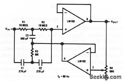
This circuit uses two LM102s to form a 60-Hz notch filter with adjustable Q. The response should fall within the shaded area of Fig. 10-42B. Remember that R4 sets the Q, not the notch frequency. Other frequencies can be selected using the equations of Fig. 10-42. (View)
View full Circuit Diagram | Comments | Reading(965)
Op_amp_notch_filter_high_Q
Published:2009/7/24 23:02:00 Author:Jessie
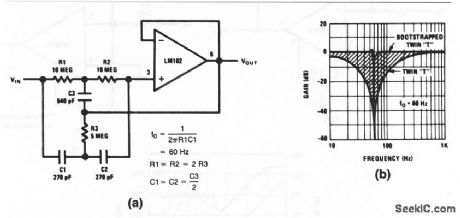
This circuit uses a single LM102 in the twin-T configuration to form a high-Q notch filter. Figure 10-42B shows the filter characteristics at 60 Hz. Other frequencies can be selected with different values, as shown by the equations. (View)
View full Circuit Diagram | Comments | Reading(1380)
Basic_multiplication_circuit
Published:2009/7/24 23:53:00 Author:Jessie
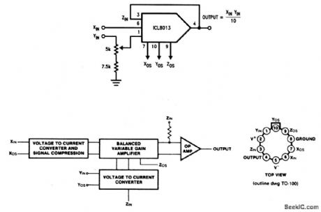
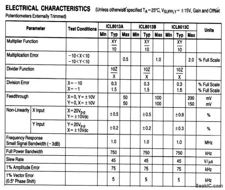
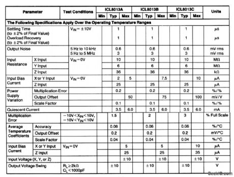
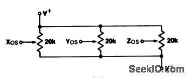
This circuit shows an ICL8013 four-quadrant multiplier connected as a basic multiplier. Figure 3-15B shows the pin connections and functional diagram. Figure 3-15C shows the electrical characteristics. Figure 3-15D shows the connections for trimming offset and feedthrough. Use the following trim procedure.
1. Set XIN= YIN= 0 V, and adjust Z0S for zero output.2. Apply a±10-V low-frequency (below 100 Hz) sweep (sine or triangle) to YINwith XIN 0 V, and adjust X0S for minimum output (chapter 5 contains several sweep-generator circuits).3. Apply the sweep signal of step 2 to XIN with YIN= 0 V, and adjust Y0s for minimum output.4. Readjust Z0s, as in step 1, if necessary.5. With XIN =10.0 Vdc, and the sweep signal of step 2 applied to YIN, adjust the gain potentiometer until the output equals YIN. This can be done with a differential scope plug-in (A + B) by inverting one signal and adjusting the gain control for (output - YIN)=0. (View)
View full Circuit Diagram | Comments | Reading(784)
Schmitt trigger circuit and its trigger characteristics
Published:2011/8/1 2:39:00 Author:Ecco | Keyword: Schmitt , trigger circuit, characteristics
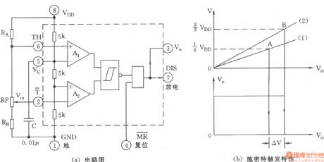
The chart shows a Schmitt trigger with adjustable threshold voltage composed of 555 time base circuit and RA, RB, RP. It could be viewed as the Schmitt trigger circuit driven by comparator. The output has two ports: One is the rectangular pulse output by pin 3; the other one is the discharging wave (external capacitor) output by pin 7 of the discharging end.
(View)
View full Circuit Diagram | Comments | Reading(1486)
SEQUENTIAL_TIMING
Published:2009/6/29 2:26:00 Author:May

By utilizing both halves of the dual timer it is possible to obtain sequential timing. By con-necting the output of the first half to the input of the second half via a.001 μF coupling capacitor, sequential timing may be obtained. Delay h is determined by the first half and t2 by the second half delay. The first half of the timer is started by momentarily connecting pin 6 to ground. When it is timed out (determined by 1.1R1C1) the second half begins. Its time dura-tion is determined by 1.1R2C2. (View)
View full Circuit Diagram | Comments | Reading(688)
Motor vehicle steering flasher 13
Published:2011/8/1 2:49:00 Author:Ecco | Keyword: Motor vehicle , steering flasher
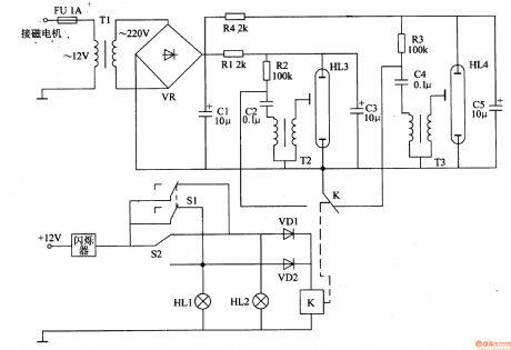
The motor vehicle steering flasher described in the example can automatically turn the flash frequently when installing on the motorcycle, it can remind the traveling vehicles to improve road safety.
The motorcycle steering circuit is composed of the power circuit, the first strobe circuit, strobe circuit and control circuit; it is shown as Figure 7-22.
Power circuitis composed ofthe fuse FU, step-up transformer Tl, rectifier bridge UR and filter capacitor Cl.
The first strobe circuit consists of resistors Rl, R2, capacitor C2, C3, and the flash tubeHL3 and trigger transformer T2.
Control circuitconsists ofthe manual switch Sl, motorcycle turn signal switch S2, the relay K and diode VDl, VD2 and so on.
Rl and R4 select thelW metal film resistors or wire wound resistors; R2 and R3 select 1/2W carbon film resistor.
Cl and C3, C5 select the electrolytic capacitors with voltagebeing 400V or more; C2 uses the polyester capacitor with the voltagein 630V or CBB capacitor.
VDl and VD2 use 1N4001 or lN4007 silicon rectifier diodes.
UR selects IA, 600V rectifier bridge reactor.
Tl uses 5W, l2/220V power transformer; m and T3 are all made of flash-specific trigger transformer.
S1 selects double-toggle switch.
HL3 and HL4 select flash tube for camera. (View)
View full Circuit Diagram | Comments | Reading(802)
Tone_detection
Published:2009/7/24 23:40:00 Author:Jessie

This circuit is similar to that of Fig. 3-9, but shows the XR-2211 (Fig.3-9C) connected as a tone detector. Q and Q are normally high and low, respectively. When a tone is present within the PLL detection band, Q and Q reverse states (for the duration of the tone). Each output (pins 5 and 6) can sink 5 mA of load current. RL1/RL2 pull-down resistors are required since both outputs are open-collector. The circuit can be optimized for any tone-detection application by the choice of R0, R0, C0, C1, and CD. For a given input-tone frequency, fs, these parameters are calculated as follows:Choose R0 in the range of 15 to 100 kΩ (arbitrary).Calculate C0 to set center frequency, f0 /fs using= C0= l/R0/fs.Calculate R1 to set bandwidth using: R1=R0(f0/▲f). Notice that the total detection bandwidth covers the frequency range of f0±▲f.Calculate C1 for a given loop-damping factor using: C1= 0.25 C0. Increasing C1 improves the out-of-band signal rejection, but increase the PLL capture time.Calculate the minimum value of filter capacitance CD using: CD (in μF) 16/capture range in Hz. Large values of CD slow response time and small CD values can result in chatter.The following values are for a tone detector with a detection band of 1 kHz ±20 Hz. R0 is an arbitrary 20 kΩ (18 kΩ 5-kΩ pot). C0=, 0.05 μF,R1=1 MΩ, C1= 0.013 μF, CD = 0.42 μF (a capture range of 38 Hz instead of 40 Hz). Fine tune the center frequency with Rx. (View)
View full Circuit Diagram | Comments | Reading(3122)
Push-pull converter circuit diagram composed of TDA4718
Published:2011/8/1 2:48:00 Author:Ecco | Keyword: Push-pull converter

The push-pull converter circuit composed of TDA4718 is shown as the chart. It uses two switching elements to do on / off work and to prevent the transformer magnetic saturation, then it can increase conversion efficiency. Transformer windings N1, N2 and N3, N4 are not symmetrical around system, and the bias point of the hysteresis loop will move, that is magnetic bias, then the output voltage increase will result in saturation. Because the transformer windings will produce stray capacitance, therefore, the higher the frequency will result in more complex inductive coupling effect between wingings.
(View)
View full Circuit Diagram | Comments | Reading(5210)
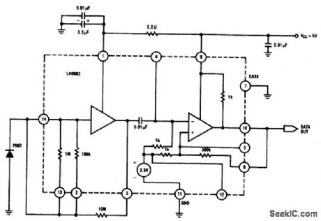
FIBER_OPTIC_RECEIVER,LOW_SENSITIVITY,2μW
Published:2009/6/29 2:08:00 Author:May

View full Circuit Diagram | Comments | Reading(619)
FIBER_OPTIC_RECEIVER,HIGH_SENSITIVITY,30nW
Published:2009/6/29 2:07:00 Author:May
View full Circuit Diagram | Comments | Reading(730)
FIBER_OPTIC_LINK
Published:2009/6/29 2:04:00 Author:May
Circuit Notes
Fiber Optic applications require analog drivers and receivers operating in the megahertz region. This complete analog transmission system is suitable for optical communication applications up to 3.5 MHz.The transmitter LED is normally biased at 50 mA operating current. The input is capacitively coupled and ranges from 0 to 5 \I, modulating the LED current from 0 to 100 mA. The re-ceiver circuit is configured as a transimpe-dance amplifier. The photodiode with 0.5 amp per watt responsivity generates a 50 mV signal at the receiver output for 1,u,W of light input. (View)
View full Circuit Diagram | Comments | Reading(2)
FIBER_OPTIC_RECEIVER,VERY_HIGH_SENSITIVITY,LOW_SPEED,3nW
Published:2009/6/29 2:00:00 Author:May
View full Circuit Diagram | Comments | Reading(638)
FIBER_OPTICS_HALF_DUPLEX_INFORMATION_LINK
Published:2009/6/29 1:58:00 Author:May
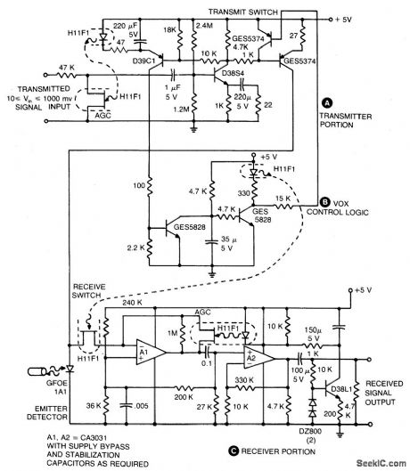
View full Circuit Diagram | Comments | Reading(694)
ERROR_TAKEOFF_REDUCES_DISTORTION
Published:2009/6/29 1:52:00 Author:May
Nonlinear distortion is reduced in singleended amplifier by producing voltage proportional to distortion and amplifying this error voltage in such a way thatit can be used to reduce distortion at output. Circuit uses 741 opamps and MJ4000 power Darlington transistors. Technique overcomes basic Iimitation of negative feedback wherein feedback loop gain decreases as frequency increases. Artide also gives variation of circuit more suitable for power amplifier, and describes circuit operation in detail.-A. M. Sandman, Reducing Amplifier Distortion, Wireless World, Oct. n974, p 367-371. (View)
View full Circuit Diagram | Comments | Reading(761)
| Pages:320/471 At 20301302303304305306307308309310311312313314315316317318319320Under 20 |
Circuit Categories
power supply circuit
Amplifier Circuit
Basic Circuit
LED and Light Circuit
Sensor Circuit
Signal Processing
Electrical Equipment Circuit
Control Circuit
Remote Control Circuit
A/D-D/A Converter Circuit
Audio Circuit
Measuring and Test Circuit
Communication Circuit
Computer-Related Circuit
555 Circuit
Automotive Circuit
Repairing Circuit