
Basic Circuit
Index 317
FOUR_QUADRANT_RATIOMETRIC
Published:2009/6/30 1:36:00 Author:May
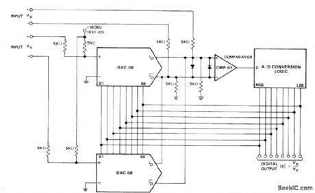


Uses Precision Monolithics DAC-08 D/A converters and CMP-01 comparator to drive successive-approximation conversion logic using REF-01 +10 V reference and 2502-type successive-approximation register. Imputs VX are connected conventionally, and inputs VY are connected in multiplying fashion. IREF for both DACs is modulated between 1 and 3 mA. Resulting output currents are differentially transformed into voltages by 5K resistors at comparator inputs and compared with VX differential input. When conversion process is complete (comparator inputs differentially nulled to less than 1/2 LSB), digital output corresponds to quotient VX/VY. Diodes are 1N4148.—J. Schoeff and D. Soderquist, Differential and Multiplying Digital to Analog Converter Applications, Precision Monolithics, Santa Clara, CA, 1976, AN-19, p 5. (View)
View full Circuit Diagram | Comments | Reading(1570)
REPETITIVE_MODE_OPERATION
Published:2009/6/30 1:35:00 Author:May
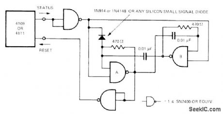
Quicker conversion is obtained in Teledyne Philbrick 4109 or 4111 A/D converter by restarting converter within a few microseconds after status signal, using surestart circuit shown. Reset pulse is fed to converter when status signal is held at low DC level. When status command is high, oscillator A-B is disabled. If reset pulse is not obeyed and status signal remains low, oscillator starts up until conversion does occur.—R.W. Jacobs, Repetitive Mode Operation for Models 4109/4111 Integrating A/D Converters, Teledyne Philbrick, Dedham, MA 1977, AN-28. (View)
View full Circuit Diagram | Comments | Reading(682)
CYCLIC_CONVERTER
Published:2009/6/30 1:29:00 Author:May

Unknown voltage is successively compared to reference voltage for determining each digital bit. After determining bit, voltage difference between unknown and reference is operated on, then sent to successive stages to determine less significant bit. Resulting digital output is in Gray-code form. Eight identical circuits are operated in cascade to provide 8-bit A/D converter having accuracy within 1 LSB and full-scale.range of 0-8 V. Circuh requires only two MC1456CG opamps per stage, with MPS6514 transistor as comparator.Switching diode CR1 is MSD6100, and CR2 is MSD6150,Other dioodes are 1N914,—JBarnes, Analog-to-Digitai Cyclic Converter, Motorola, Phoenix, AZ, 1974, AN-557、P 7. (View)
View full Circuit Diagram | Comments | Reading(2181)
0_10_V_ANALOG_INPUT
Published:2009/6/30 1:25:00 Author:May
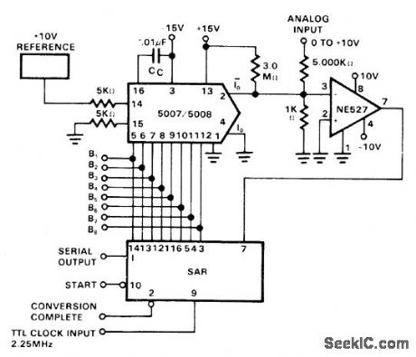
Used to provide digital input to computer for processing and storage of analog signals. Requires only three ICs in addition to external +10 V reference and 2.25-MHz TTL clock. Successive-approximation register (SAR) can be Motorola MC1408 or equivalent. For continuous conversions, connect pins 10 and 2 of SAR.— Signetics Analog Data Manual, Signetics, Sunnyvale, CA, 1977, p 677-685. (View)
View full Circuit Diagram | Comments | Reading(1591)
AUDIO_FILTERS_FOR_SNR_MEASUREMENT
Published:2009/6/30 Author:May
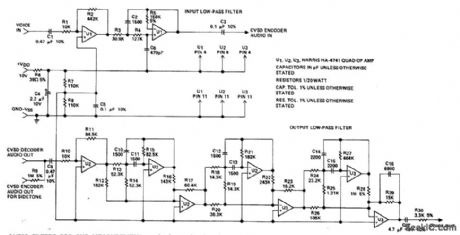
Used in checking performance of Harris HC-55516/55532 haff-duplex modulator-demodulator systems for converting voice signals into s rial NRZ digital data and reconverting that data back to voice. Supply required for opamp sections is ±15 V. Response of input filter is down 3 dB at 3 kHz and is down 20 dB at 9 kHz. Response of output filter is flat up to 3 kHz and down more than 45 dB from 3.8 kHz to 100kHz.- Linear & Data Acquisition Products, Harris Semiconductor,Melbourne,FL,Vol.1,1977,p 5-10. (View)
View full Circuit Diagram | Comments | Reading(739)
IMPROVED_BAXANDALLCONT_ROL
Published:2009/6/29 23:57:00 Author:May
Uses separate effect″controls for bass and treble tolimit maxlmum degree of boost and cut obtainable from bass and treble controls,R18 controls effect for bass and R21 for treble. Circuit has unity gain with controls set flat. Article gives response curves and describes operation of cir cult in detail-M,V,Thomas、Baxandall ToneControl Revisited、Wireless World, Sept,1974,p341-343. (View)
View full Circuit Diagram | Comments | Reading(2315)
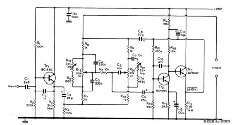
VIDEO_COMPRESSOR
Published:2009/6/29 23:56:00 Author:May
Nonlinear function amplifier IC-2 compresses video input signals as required to compensate for inefficient quantization where there are too many levels for small signals and too few levels for large signals. Designed to feed 6-bit analog-to-digital converter, IC-1 attenuates input -20 dB and shifts level.Output of IC-2 is amplified by IC-3 to voltage range comparable to that of input signal. IC-4 acts as temperature compensator and output level shifter. R7 nulls small output offsets.—J.B. Frost, Non-Linear Function Amplifier, EEE Magazine, March 1971, p 78. (View)
View full Circuit Diagram | Comments | Reading(719)
SPEECH_FlLTER
Published:2009/6/29 23:56:00 Author:May
High-pass and low pass filters in cascade provide comer frequencies of 300 and 3000 Hz for limiting audio bandwidth to speech frequencies. Rolloff beyond corners is -40 dB per decade. Input-to-output gain is 1.- Audio Handbook, National Semiconductor, Santa Clara, CA, 1977, p 2-49-2-52. (View)
View full Circuit Diagram | Comments | Reading(1254)
10_BIT_ACCURACY
Published:2009/6/29 23:55:00 Author:May
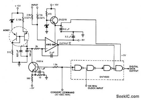
Single-slope A/D converter gives high-speed conversion of DC input voltage to digital data output. For 0-10 V input, 1024 pulses of 100-MHz clock appear at full scale and 512 at half scale. When command pulse is applied, 2N914 transistor resets 1000-pF capacitor (820 and 180 in parallel) to 0 V. Capacitor begins to charge linearly on falling edge of command pulse, to 2.5 V. 10-μs ramp is applied to AMD686 for comparison with unknown voltage. Output of opamp is pulse whose width is proportional to input voltage and can therefore be used to gate 100-MHz clock.—J. Williams, Low-Cost, Linear A/D Conversion Uses SingleSlope Techniques, EDN Magazine, Aug. 5, 1978, p 101-104. (View)
View full Circuit Diagram | Comments | Reading(1112)
ASYMMETRICAL_ACTIVE_CROSSOVER
Published:2009/6/29 23:51:00 Author:May
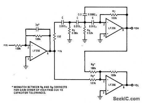
High-pass and low-pass active filters using National LF356 opamps are asymmetrical about 500-Hz crossover point,Sum of filter output voltages is always constant and equaltounity,Rolloff of low-pass filter is only-6 dB peroctave、as compared to-18 dB per octave for high-pass filter,-″Audio Handbook″ National semiconductor, Santa Clara,GA,1977、p 5-1-5-7. (View)
View full Circuit Diagram | Comments | Reading(1871)
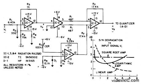
Basic_division_circuit
Published:2009/7/24 23:57:00 Author:Jessie
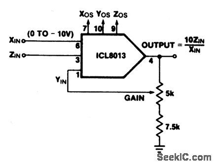
This circuit shows an ICL8013 (refer to Fig. 3-15) connected as a basic divider. Use the following trim procedure.1. Set the trim pots (Fig. 3-15D) at mid-scale by adjusting the voltage on pins 7, 9, and 10 for 0 V.2. With ZIN= 0V, trim Z0s to hold the output constant as XIN is varied from -10 V through -1 V.3. With ZIN= 0 V and XIN =10.0 V adjust Yos for zero output voltage.4. With ZIN=XIN (and/or ZIN =-XIN) adjust Xos for minimum worst-case variation of output as XIN is varied from -10 V to -1 V.5. Repeat steps 2 and 3 if step 4 requires a large initial adjustment.6. With ZIN = XIN (and/or ZIN = -XIN), adjust the gain control until the output is the closest average around +10.0 V (-10 V for ZIN =-XIN) as XIN is varied from -10 V to-3 V. (View)
View full Circuit Diagram | Comments | Reading(736)
ACTIVE_RC_FILTER_FOR_FREQUENCIES_UP_TO_150_kHz
Published:2009/6/29 23:03:00 Author:May
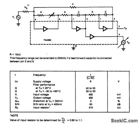
View full Circuit Diagram | Comments | Reading(648)
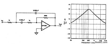
TUNABLE_ACTIVE_FILTER
Published:2009/6/29 23:01:00 Author:May
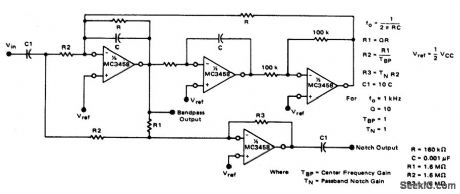
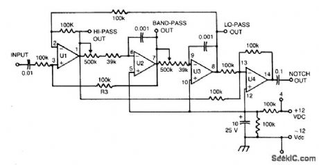
Circuit NotesThe high-pass and low-pass outputs cov-ering the range of 300 Hz to 3000 Hz have been summed in the fourth op amp to provide a notchoutput. The potentiometers must have a re-verse log taper. Fixed-frequency active filter center frequency is1 kHz, with a Q of 50. (View)
View full Circuit Diagram | Comments | Reading(940)
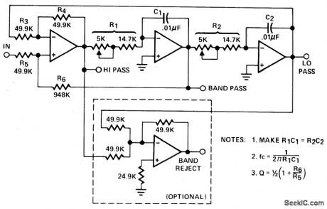
SECOND_ORDER_STATE_VARIABLE_FILTER(1_kHz,Q=10)
Published:2009/6/29 22:56:00 Author:May
View full Circuit Diagram | Comments | Reading(971)
BIQUAD_FILTER
Published:2009/6/29 22:54:00 Author:May
Circuit Notes
The biquad filter, while appearing very similar to the state-variable filter, has a bandwidth that is fixed regardless of center frequency. This type of filter is useful in applications such as spectrum analyzers, which require a filter with a fixed bandwidth. (View)
View full Circuit Diagram | Comments | Reading(1171)
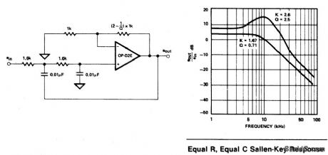
EQUAL_COMPONENT_SALLEN_KEY_LOW_PASS_FILTER
Published:2009/6/29 22:53:00 Author:May
View full Circuit Diagram | Comments | Reading(755)
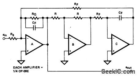
FILTER_NETWORKS
Published:2009/6/29 22:50:00 Author:May
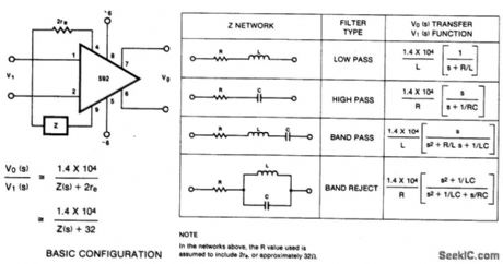
View full Circuit Diagram | Comments | Reading(689)
AUDIO_SWITCHING_GATE
Published:2009/6/29 22:49:00 Author:May
Can be used with programmed channel selectors, as required in music synthesis for controlling audio signals by means of TTL levels. DC offset at output is negligible when gate is off, simplifying design of subsequent stages. Use logic 1 (+5 V) to open gate, and logic 0 (0 V) to close it.-L. Cook, Analogue Gate with No Offset, Wireless World, Feb.1975, p 93. (View)
View full Circuit Diagram | Comments | Reading(909)
500_Hz_SALLEN_KEY_BANDPASS_FILTER
Published:2009/6/29 22:48:00 Author:May
View full Circuit Diagram | Comments | Reading(858)
PANNING_MIXER_POT
Published:2009/6/29 22:48:00 Author:May
Circuit gives best possible approach to sine law so A2 = B2 is constant for all positions of wiper. Calculated error is less than n dB over full range of wiper. Use wirewound pot to minimize crosstalk.-J. Dawson, Single Gang Pan-Pot, Wireless World, Feb 1976,p78. (View)
View full Circuit Diagram | Comments | Reading(951)
| Pages:317/471 At 20301302303304305306307308309310311312313314315316317318319320Under 20 |
Circuit Categories
power supply circuit
Amplifier Circuit
Basic Circuit
LED and Light Circuit
Sensor Circuit
Signal Processing
Electrical Equipment Circuit
Control Circuit
Remote Control Circuit
A/D-D/A Converter Circuit
Audio Circuit
Measuring and Test Circuit
Communication Circuit
Computer-Related Circuit
555 Circuit
Automotive Circuit
Repairing Circuit