
Basic Circuit
Index 319
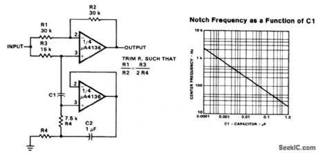
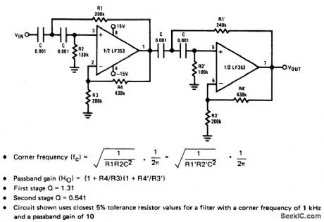
1_kHz_BANDPASS_ACTIVE_FILTER
Published:2009/6/29 21:25:00 Author:May
View full Circuit Diagram | Comments | Reading(667)
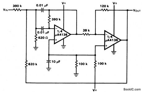
NOTCH_FILTER_USING_THE_μA4136_AS_A_GYRATOR
Published:2009/6/29 21:08:00 Author:May
View full Circuit Diagram | Comments | Reading(831)
REJECTION_FILTER
Published:2009/6/29 21:07:00 Author:May
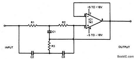
Circuit Notes
This narrowband filter using the 741 operational amplifier can provide up to 60 dB of rejection. With resistors equal to 100 K and capacitors equal to 320 pF, the circuit will reject 50 Hz. Frequencies within the 1 Hz to 10 kHz may be rejected by selecting components h accordance with the formula∶F=1/2πRCTo obtain rejections better than 40 dB,reslstors should be matched to 0.1%and capacitors to 1%. (View)
View full Circuit Diagram | Comments | Reading(878)
SOLAR_POWER_BACKUP
Published:2009/6/29 21:05:00 Author:May
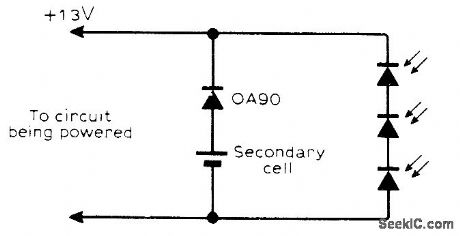
If solar-cell voltage drops 0.2 V below battery voltage, circuit is powered by storage cell feeding through forward-biased 0A90 or equivalent germanium diode. When solar-cell voltage exceeds that of battery, battery is charged by approximately constant reverse leakage current through diode. Battery can be manganese-alkaline type or zinc-silver oxide watch-type celL-M. Hadley Automatic Micropower Battery Charger, Wireless World, Dee. 1977, p 80. (View)
View full Circuit Diagram | Comments | Reading(985)
HIGH_Q_NOTCH_FILTER
Published:2009/6/29 20:58:00 Author:May

Circuit NotesA shows atwin-T network connected to anLM102 to form a high Q, 60 Hz notch filter, Thejunction of R3 and C3, which t normally connected to ground, is bootstrapped to the outputof the follower, Because the output of the follower is a very low impedance, neither the depth nor the frequency of then.tch change; however, the Q is raised In proportion to thealηount of signal fed back to R3 and C3. Bshows the response ofa normal twin-T and theresponse with the foilower added. (View)
View full Circuit Diagram | Comments | Reading(0)
45_MHz_NOTCH_FILTER_
Published:2009/6/29 20:56:00 Author:May
Circuit NotesComponenc value sensitivity is extremely critical, as are temperature coefficients and matching ofthe components. Best performa,ce is attained when perfectly matched components are used and when the gain of the amplifier is unity.To illustrate,the quality factor Q is very high as amplifier gam approaches1 with all components matched(In fact,theoretically it approaches co)but decreases toabout 12.5 with the amplifier gain at 0.98. (View)
View full Circuit Diagram | Comments | Reading(706)
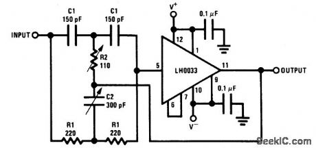
TUNABLE_NOTCH_FILTER_TO_SUPPRESS_HUM
Published:2009/6/29 4:41:00 Author:May
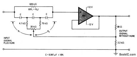
Circuit Notes
This narrow-stop-band filter can be tuned by the pot to place the notch at any frequency from 45 to 90 Hz. It attenuates power-line hum or other unwanted signals by at least 30 dB.Because the circuit uses wide-tolerance parts, it is inexpensive to build. (View)
View full Circuit Diagram | Comments | Reading(777)
FOURTH_ORDER_HIGH_PASS_BUTTERWORTH_FILTER
Published:2009/6/29 4:38:00 Author:May
View full Circuit Diagram | Comments | Reading(0)
10_kHz_SALLEN_KEY_LOW_PASS_FILTER
Published:2009/6/29 4:36:00 Author:May
View full Circuit Diagram | Comments | Reading(701)
DIGITALLY_TUNED_LOW_POWER_ACTIVE_FILTER
Published:2009/6/29 4:35:00 Author:May
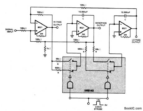
Circuit NotesConstant gain, constant Q, variable frequency filter which provides simultaneous low-pass, bandpass, and high-pass outputs.With the component values shown, center frequency will be 235 Hz and 23.5 Hz for high and low logic inputs respectively, Q=100, and gain=100.
fn=center frequency =1/2πRC (View)
View full Circuit Diagram | Comments | Reading(782)
FIVE_POLE_ACTIVE_FILTER
Published:2009/6/29 4:30:00 Author:May
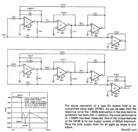
The above realization of a type D3 receive filter is accompished using eight OP-08's. As can be seen from 1he response curve the >30dB attenuation in the stop band re-qu jrement has been met. In addition, thenoise performance of <0dBHn has been measured. One of the unique features of the OP-08 is ils low supply current of 600μA maximum Thus the total supply dralrl for all eight op amps is only 4.8mA. (View)
View full Circuit Diagram | Comments | Reading(705)
LATCHING_GATES
Published:2009/6/29 4:01:00 Author:May
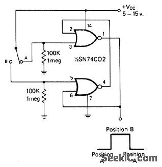
SN74C02 quad two-input NOR gate forms latching circuit in which first noise pulse produced by switch latches circuit, making it immune to contact bounce.—I. Math, Bounceless Switch, CQ, July 1976, p 50. (View)
View full Circuit Diagram | Comments | Reading(1071)
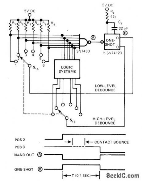
BOUNCE_FREE_INTERLOCKING
Published:2009/6/29 4:01:00 Author:May
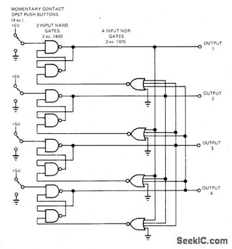
Arrangem ent provides low-cost equivalent of mechanically inteelocked switch assembly, while providing TTL compatibility and freedom from switch bounce. Momentary pressing of any pushbutton restores its associated RS flip-flop to normal and makes output of that channel high. Arrangement uses cross-coupled two-input NAND gates for each flip-flop, connected so each actuation produces an output and resets all other flip-flops. If two or more buttons are pushed simultaneously, all their channels will go high, but only last one released will stay on. Any number of channels may be added.—B.Brandstedt, Digital Interlocking Switch is Inex-pensive to Build, EDN Magazine, Dec. 15, 1972, p 42. (View)
View full Circuit Diagram | Comments | Reading(862)
BOUNCELESS_MAKE_BREAK
Published:2009/6/29 4:00:00 Author:May
Circuit eliminates switch bounce problems during closing as well as opening. When switch is closed, Q output of flip-flop goes to logic 1 for delay period determined by RC time constant. Releasing switch operates NAND gate, making its output go to logic 1. This charges C through R until reset level is reached. Flip-flop then resets, changing Q output to logic 0. Values for R and C are chosen according to bounce duration of switch used. Fortypical 1-ASPST switch, 10,000 ohms and 0.41 μF were used.—L. F, Walsh and T. W. Hill, Make-and-Break Bounceless Switching, EDN|EEE Magazine, July 15, 1971, p 49. (View)
View full Circuit Diagram | Comments | Reading(786)
DEBOUNCING_WITH_COUNTER
Published:2009/6/29 3:59:00 Author:May
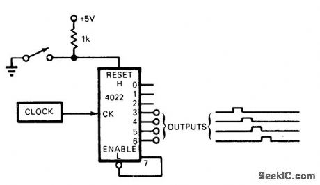
Circuit uses CMOS counteridecoder with any inexpensive 200-Hz or higher clock such as CMOS two-gate oscillator or 555 timer. Signal to be debounced is fed directly to reset input of counter, with no preconditioning. When contact is made by switch, counter unclears and starts counting up. Each bounce of contact resets counter, so it cycles between states 0 and 1 until contacts settle. Counter then delivers clean nonoverlapping pulses to remaining output lines, any of which may be used as conditioned output signal.When counter reaches state 7, it inhibits itself to prevent repeated pulsing of output lines. When switch is opened, cycling action is repeated during bounces, with output never going higher than state 1. After bouncing, counter is held in clear state ready for next closing.—L. T. Hauck, Solve Contact Bounce Problems Without a One-Shot, EDN Magazine, Sept, 5, 1975, p 80 and 82 (View)
View full Circuit Diagram | Comments | Reading(828)
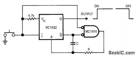
ROTARY_SWITCH_DEBOUNCE
Published:2009/6/29 3:50:00 Author:May
Outputs from mono (one-shot) provide common retums for rotary switch. Multi-input NAND gate, tied to normally high signals from one deck of rotary swhch, instantly detects opening of one contact and triggers mono. Mono then simulates open contact for interval determined by values used for R7 and C1; for values shown, delay is 400 ms.—E. S. Peltzman, Circuit Eliminates Rotary-Switch Bounce Problems, EDN Magazine, April 20, 1978, p 132. (View)
View full Circuit Diagram | Comments | Reading(1136)
BOUNCELESS_ISOLATOR
Published:2009/6/29 3:48:00 Author:May

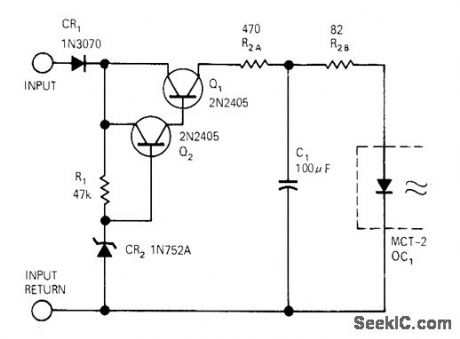
Integrating filter C1-R2 eliminates effects of contact bounce that may be superimposed on digital input signal feeding optoisolator. Photodiode in optoisolator drives Schmitt trigger that makes output to TEL circuits change state when LED is turned on by input signaL—C. E. Mitchell, Optical Coupler and Level Shifter, EDN|EEE Magazine, Feb.1, 1972, p 55. (View)
View full Circuit Diagram | Comments | Reading(748)
Protective principle circuit diagram
Published:2011/8/1 2:23:00 Author:Ecco | Keyword: Protective principle
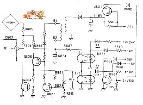
Protective circuitry: According to figure 1, when the supply is in start state, the electricity can be connected by R805, R858. On the one hand, when the output voltage is rising, the D811 can reach the state of starting by the IF1 of R864. D836 is later than D811, it appears the state of start when the current flows to LF2 from F, B, T 24. Then, IF1 produces firstly, IF2 is later, after Tr1 appears the state of ON , Tr2 can be switched on. When the burden is unusual, for example, it can produce overcurrent, and when base current of Q805 produces, Q805 appears the state of ON . When IF1 of D811 is cut-off, Tr1 will be the state of OFF . Q827 appears the state of breakover by VTr1 when through D823. Simultaneously, Q826 is also in starting state. The collector current Ic make the Q804 is in staring state, and the shunt of Ic passes R854 that make of Q827 base maintaining current, Q827, Q826 keep in the staring state. With the Ic, Q804 is in the staring state, the base of Q1 locating inside of IC802 connects 3 and then connects to the earth, the supply will stop working. When appearing short circuit, the circumstances are as below: a. 50V short circuit: D837 is on, D811 is stop. b. 115V short circuit: D830 is on, D811 is stop. c. 16V short circuit: the current of D811 isn't provided by R864, D811 will stop.
(View)
View full Circuit Diagram | Comments | Reading(538)
45_W_CLASS_B
Published:2009/6/29 3:08:00 Author:May
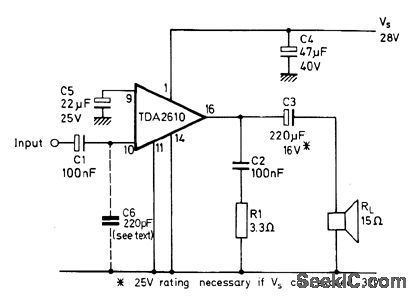
Mullard TDA2610 drives 15-ohm loudspeaker with total harmonic distor-tion of lessthan 1%. Supply is 28V ±10%. Net-work C2-R1 ensures stability with inductive Ioad.- Audio Power Amplifier TDA2610, Mullard, London, 1976, Technical Note 35, TP1541. (View)
View full Circuit Diagram | Comments | Reading(1204)
FEED_FORWARD_CORRECTION
Published:2009/6/29 3:05:00 Author:May
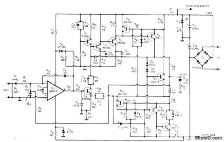
Circuit re-duces distortion caused by nonlinearity of out-put power transistors by deriving error com ponent that bypasses these transistors.Technique used is known as current dumping.Article describes operating principle in detail.Circuit shown gives application to commercial amplifier (Quad 405), in which midfrequency distortion is only about 0.005%. Features in-clude elimination of adjustments, alignment procedures and thermal problems during entire life of amplifier,-P.J. Walker, Current Dumping Audio Amplifier,Wireless World,Dec.1975,p 560-562 (View)
View full Circuit Diagram | Comments | Reading(2224)
| Pages:319/471 At 20301302303304305306307308309310311312313314315316317318319320Under 20 |
Circuit Categories
power supply circuit
Amplifier Circuit
Basic Circuit
LED and Light Circuit
Sensor Circuit
Signal Processing
Electrical Equipment Circuit
Control Circuit
Remote Control Circuit
A/D-D/A Converter Circuit
Audio Circuit
Measuring and Test Circuit
Communication Circuit
Computer-Related Circuit
555 Circuit
Automotive Circuit
Repairing Circuit