
Basic Circuit
Index 312
2_1_2_DIGIT_INPUT_FOR_199_COUNT
Published:2009/6/30 3:08:00 Author:May
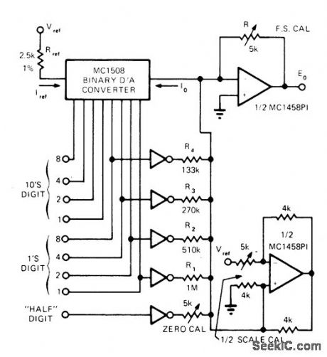
Addition of 1/2-digit circuit to basic 2-digit BCD DAC increases countfrom 99 to 199,Circuit sequencesto 99 while 1/2-digitsection of MC14009 hex two-output NOR gate has low output, and goes through steps 100 to 199 while 1/2-digit output is high Reference voltage is 5.0 V. Calibration procedure is given.—T.Henry,Binary D/A Converters Can Provide BCD-Coded Conversion,EDN Magazine, Aug.5, 1973, p 70-73. (View)
View full Circuit Diagram | Comments | Reading(1137)
2_DIGIT_BCD
Published:2009/6/30 3:07:00 Author:May
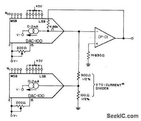
Output current of Precision Monolithics DAC-100 D/A converter can be adjusted to exactly desired value with 200-ohm pot for each DAC; adjustment is made with input of all 0s. Circuit can be expanded to 3 digits by adding third DAC and adding 99 to current divider.— 8 & 10 Bit Digital-to-Analog Converter, Precision Monolithics, Santa Clara, CA, 1977, DAC-100, p 5. (View)
View full Circuit Diagram | Comments | Reading(0)
2_DIGIT_BCD_INPUT
Published:2009/6/30 3:01:00 Author:May
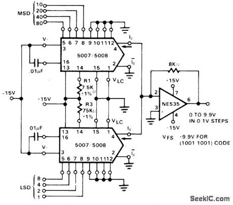
Each Signetics 5007/5008 multiplying D/A convener serves one digh of input voltage to give output current that is product of digital input number and input reference current,Opamp combines currents and converts them to analog output voltage proportional to digital input value.—Signetics Analog Data Manual, Signetics, Sunnyvale, CA, 1977, p 677-685. (View)
View full Circuit Diagram | Comments | Reading(719)
6_BITS_TO_ANALOG
Published:2009/6/30 2:59:00 Author:May
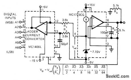
Uses Motorola MC1723G voltage regulator to provide reference voltage and opamp for MC1406L 6-bit D/A converter. Output cument can be up to 150 mA. Full-scale output is about 10 V, but can be boosted as high as 32V by increasing value of R2 and increasing +15 V supply proportionately to maximum of 35 V.—D. Aldridge and K. Huehne, 6-Bit D/A Converter Uses Inexpensive Components, EDN Magazine, Dec. 15, 1972, p 40-41. (View)
View full Circuit Diagram | Comments | Reading(791)
Low_offset_12th_order_max_flat_low_pass_filter
Published:2009/7/24 13:09:00 Author:Jessie
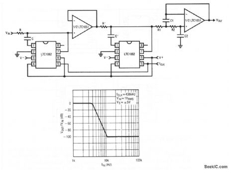
This circuit shows a 12th-order filter that uses two LTC1062s and a precision dual op amp. Figure 7-16B shows the frequency response for the following values: fc=4 kHz, R=59 kΩ, C=0.001μF, R'=5.7 kΩ, C'=0.01 μF, R1=R2=39.8 kΩ, C1=2000 pF, C2=500 pF, fclock=438 kHz. Linear Technology Corporation, Linear Applications Handbook, 1990, p. AN20-8, -9. (View)
View full Circuit Diagram | Comments | Reading(655)
Cascaded_IC_low_pass_filters
Published:2009/7/24 13:07:00 Author:Jessie
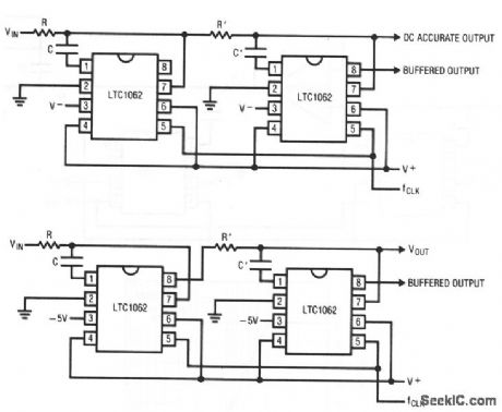
Figure 7-15A shows two LTC1062 filters where the second input is taken directly from the dc-accurate output of the first filter. The recommended ratio of R'/R is about 117/1, 1/(6.28RC) should equal fc/1.57, and 1/(6.28R'C') should equal fc/1.6 when the filters are cascaded (Fig. 7-15A). For example, for an fc of 4.16 kHz, the clock should be 416 kHz, and R=909 Ω, R'=107 kΩ, C=0.066 pF, and C'=574 pF. Figure 7-15B shows cascaded filters where the second input is taken from the buffered output of the first filter. The recommended values for R and C are determined by: 1/(6.28RC) =fc/1.59 and 1/(6.28R'C')=fc/1.64 when the filters are cascaded as shown in Fig. 7-15B. For example, for an fc of 4kHz, the values should be: R=97.6 kΩ, C=616 pF, R'=124 kΩ, and C'=508 pF. Linear Technology Corporation, Linear Applications Handbook, 1990, p. AN20-7. (View)
View full Circuit Diagram | Comments | Reading(679)
IC_Iow_pass_filter
Published:2009/7/24 13:05:00 Author:Jessie
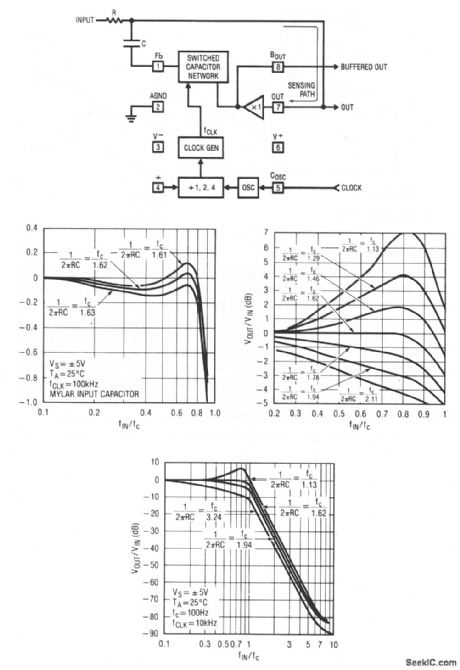
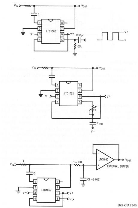
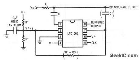

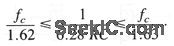


Figure 7-14A shows the architecture and basic connections for an LTC1062 low-pass filter (similar to a 5th-order Butterworth). The cutoff frequency fc (at the -3-dB point) is determined by the values of R and C, with the relationship:
The clock frequency should be 100 times fc,. Figure 7-14B shows the passband response for values of 1/(6.28RC) near fc/1.62. Figures 7-14C and 7-14D are similar, but with a wider range of values. Figure 7-14D shows the LTC1062 operated from a single supply and an external CMOS clock signal. Figure 7-14F shows the LTC1062 operated with the internal clock. If COSC is 8500 pF and a 50-kΩ pot is connected to pin 5, the clock frequency can be adjusted from 500 Hz to 3.3 kHz (providing for an fc of 5 to 33 Hz). Figure 1-14G shows how an extemal buffer can be connected to the LTC1062 to eliminate clock feedthrough and improve the high-frequency attenuation floor. Figure 7-14H shows how the LTC1062 can be operated from a single supply , Linear Technology Corporation, Linear Applications Handbook, 1990, p. AN20-1, -2, -3, -4.
(View)
View full Circuit Diagram | Comments | Reading(887)
Single_2nd_order_filter_section
Published:2009/7/24 12:59:00 Author:Jessie
The MAX274/275 continuous-filter architecture uses a four-amplifier state-variable design. The on-chip capacitors and amplifiers, together with external resistors, form cascaded integrators with feedback to provide simultaneous low-pass and bandpass filtered outputs. The low-pass and bandpass frequencies, as well as filter Q, are determined by external resistor values, using the equations shown. No external capacitors are needed. On-chip capacitors are factory trimmed to provide better than 1% pole-frequency accuracy over the temperature range. ±1%-tolerance resistors provide ±2%-accurate pole frequencies. Accurate filter Qs can also be obtained by compensating for amplifier bandwidth limitation using the graphs that are provided on the data sheet. Maxim, 1992, Applications and Product Highlights, p. 7-3. (View)
View full Circuit Diagram | Comments | Reading(1325)
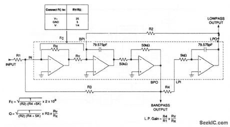
Power_on_reset_generator
Published:2009/7/24 12:41:00 Author:Jessie
This circuit uses both sections of an LT1018 to reset a digital system after supply turn-on. When supply power is applied, the 5-V rail comes up. The LT1004 clamps at 1.2 V and the C1A noninverting input ramps at a time constant that is determined by the 0.05% resistors and the 0.1-μF capacitor. When the C1A noninverting input ramps beyond the LT1004 potential, the C1A output goes high and delivers a differentiated pulse to the C1B inverting input. The C1B output goes low for a period that is determined by the 0.01-μF/680-kΩ differentiator. The 1N914 gives quick reset for the 0.1-μF capacitor, and the Schottky diode clips differentiator-caused negative voltages at the C1B input. The turn-on threshold (4.8 V in this case) is set by the ratio of the 0.5% resistors. The output-pulse delay time is controlled by the 0.1-μF capacitor, which can be varied. Similarly, the RC combination at C1B sets output pulse width, and can be varied. The LT1018 1.2-V minimum supply voltage prevents spurious output during supply power-up. Linear Technology, Linear Applications Handbook, 1990, p. AN31-10. (View)
View full Circuit Diagram | Comments | Reading(934)
Watchdog_timer_to_prevent_lock_up
Published:2009/7/24 12:39:00 Author:Jessie
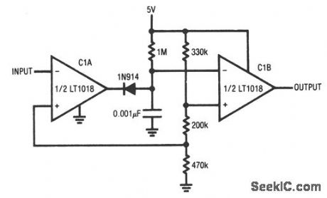
This circuit uses both sections of an LT1018 to prevent lock-up in processor-based systems. Such lock-up can occur if the system misses an instruction because of transients in hardware or software, and usually results in loss of pulses somewhere in the system. This circuit issues a reset command in response to such a pulse loss. Normally, a pulse train appears at the circuit input and causes the C1A output to pulse low. The diode path discharges the 0.01-μF capacitor each time the C1A output goes low. Interruption of the input pulse train (after the 7th vertical division) allows the capacitor to charge beyond the C1B threshold, and triggers C1B low. This pulse can be used to reset the system (applied to the microprocessor RST input). The C1B negative-input RC values can be adjusted to accommodate various input pulse-repetition rates. Linear Technology, Linear Applications Handbook, 1990, p. AN31-10. (View)
View full Circuit Diagram | Comments | Reading(682)
Full_duplex_RS_232_that_uses_negative_charge_storage
Published:2009/7/24 12:36:00 Author:Jessie
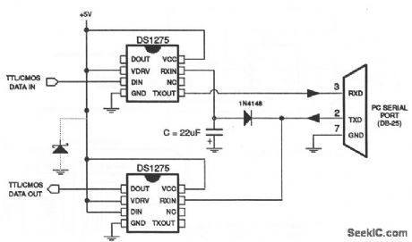
This circuit shows two DS1275 chips to provide full-duplex operation for both TTL and CMOS. Dallas Semiconductors, Product Data Book, 1992/1993, p. 10-113. (View)
View full Circuit Diagram | Comments | Reading(586)
Hand_held_line_powered_RS_232_C_transceiver
Published:2009/7/24 12:34:00 Author:Jessie
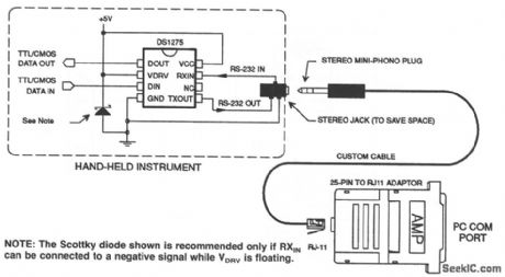
This circuit shows a DS1275 as a hand-held IRS-232-C transceiver using a stereo mini-jack and 25-pin to RK11 adaptor. Notice that the DS1275 accommodates both TTL and CMOS data. Dallas Semiconductors, Product Data Book, 1992/1993, p. 10-113. (View)
View full Circuit Diagram | Comments | Reading(724)
Digital_power_switching_for_SRAMs
Published:2009/7/24 12:29:00 Author:Jessie
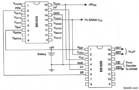
This circuit shows DS1236 and DS1336 chips that are used to provide power switching. When larger operating currents are required in a battery-backed system, the 5-V supply and battery-supply switches within the DS1236 cannot be large enough to support the required load through VCCO with a reasonable voltage drop. When such large currents are required, the PF and PF outputs are provided to gate external power switching devices. Power to the load is switched from VCC to battery on power-down, and from battery to VCC on power-up. The DS1336 uses the PF to switch between VBAT and VCC. The load applied to the PF pin from the extemal switch is supplied by the battery. Thus, if a discrete switch is used, this load should be considered when sizing the battery. Dallas Semiconductors, Product Data Book, 1992/1993, p. 10-77. (View)
View full Circuit Diagram | Comments | Reading(615)
Basic_squaring_circuit
Published:2009/7/24 23:57:00 Author:Jessie
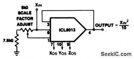
This circuit shows an ICL8013 (refer to Fig. 3-15) connected as a basic ) squaring circuit(with can also be used as the basis for a frequency doubler). (View)
View full Circuit Diagram | Comments | Reading(833)
FOUR_CHANNEL_BCD
Published:2009/6/30 2:56:00 Author:May
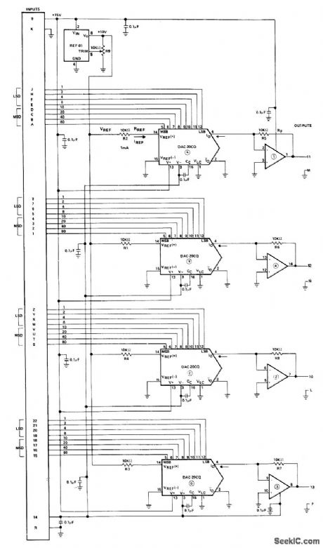
Uses four Precision Monolithics DAC-20CQ 2-digit BCD D/A con verter, OP-11FY precision quad opamp, and REF-01HJ +10 V voltage referenceto convert 2-digit BCD input coding to proportional analog 0 to +10 V output for each of four channels.Same configuration will handle binary inputs, as covered in application note. For output range of 0 to +5 V, change voltage reference to REF-02.—D. Soderquist, Low Cost Four Channel DAC Gives BCD or Binary Coding, Precision Monolithics, Santa Clara, CA, 1977, AN-26, p 3. (View)
View full Circuit Diagram | Comments | Reading(698)
NEON_BLINKER
Published:2009/6/30 2:52:00 Author:May
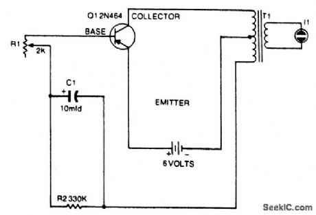
Circuit NotesThe universal output transformer and the transistor form a low-frequency oscillator. The rate of flashing of the neon bulb is determined by potentiometer R1. (View)
View full Circuit Diagram | Comments | Reading(995)
8_BIT_BINARY_TO_PROCESS_CURRENT
Published:2009/6/30 2:50:00 Author:May
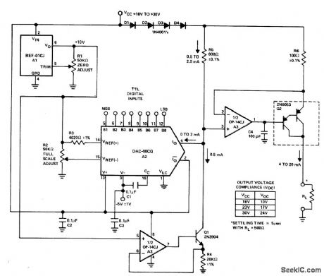
Usesonly three Precision Monolithics ICs operating from -5V and +23 V supplies to convert 8-bit binary digital input to process current in range of 4-20 mA. Fixed current of 0.5 mA is added to DAC output current varying between 0 and 2 mA, with resulting total current multiplied by factor of 8 to give up to 20 mA through 500-ohm load,—D Soderquist, 3 IC 8 Bit Binary Digital to Process Current Converter with 4-20 mA Output, Precision Monolithics, Santa Clara, CA, 1977, AN-21. (View)
View full Circuit Diagram | Comments | Reading(1541)
Basic_crystal_filter
Published:2009/7/24 12:57:00 Author:Jessie
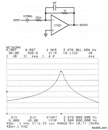
This circuit replaces the ceramic element of Fig. 7-10 with a 3.57-MHz quartz crystal. Figure 7-12B shows almost 30-dB attenuation only a few kHz on either side of resonance. Linear Technology Corporation, 1991, AN47-48/49. (View)
View full Circuit Diagram | Comments | Reading(784)
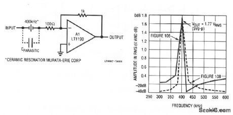
Piezo_ceramic_based_filter_with_differential_network
Published:2009/7/24 12:56:00 Author:Jessie
This circuit is an improved version of the Fig. 7-10 circuit. With the Fig. 7-11 circuit, a portion of the input is fed to the noninverting input of A1. The RC network at this input looks like the ceramic-resonantor impedance when it is off null, As a result, A1 sees similar signals for out-of-band inputs. The high-frequency roll-off of Fig. 7-11 is smooth and about 20 dB deeper than the Fig. 7-10 filter at 475 kHz. The low-frequency side of resonance has similar characteristics at 375 kHz and below. Linear Technology Corporation, 1991, AN47-48. (View)
View full Circuit Diagram | Comments | Reading(658)
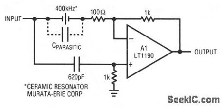
Basic_piezo_ceramic_based_filter
Published:2009/7/24 12:55:00 Author:Jessie
This circuit is a highly selective bandpass filter that uses a resonant ceramic element and a single amplifier. The ceramic element looks like a high impedance off the resonant frequency (400 kHz, in this case). At resonance, the ceramic element has a low impedance, and A1 responds as an inverter with gain. As shown, the ceramic element has stray or parasitic capacitance that causes a slight rise in output at frequencies above 425 kHz. Typically, the A1 output is down about 20 dB at 300 kHz and 40 dB at 425 kHz. The parasitic capacitance can be minimized with a differential network (Fig. 7-11). Linear Technology Corporation, 1991, AN47-48. (View)
View full Circuit Diagram | Comments | Reading(702)
| Pages:312/471 At 20301302303304305306307308309310311312313314315316317318319320Under 20 |
Circuit Categories
power supply circuit
Amplifier Circuit
Basic Circuit
LED and Light Circuit
Sensor Circuit
Signal Processing
Electrical Equipment Circuit
Control Circuit
Remote Control Circuit
A/D-D/A Converter Circuit
Audio Circuit
Measuring and Test Circuit
Communication Circuit
Computer-Related Circuit
555 Circuit
Automotive Circuit
Repairing Circuit