
Basic Circuit
Index 306
MACHINE_VISION_ILLUMINATION_STABILIZER
Published:2009/7/1 1:13:00 Author:May
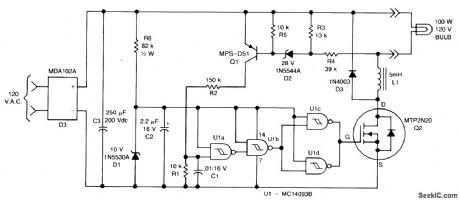
The combination of Q1, Q2 and U1 form a hysteresis oscillator to stabilize lamp illumination. In operation, full wave bridge D3 operates directly from the ac line to sup-ply unregulated dc to the lamp and also to the 10 V zener that provides power to the quad CMOS Schmitt trigger, U1. When the lamp supply exceeds 115 V, Q1 is turned ON, charging Ct through R2 to raise the input to Ula past the positive-going logic thresh-old. This drops the output voltage at Ulc and Uld, which drives the gate of Q2, turning it OFF. Current then decays through the lamp, L1 and D3 until the lamp voltage falls below 115 V, at which time Q1 turns OFF and the cycle repeats. (View)
View full Circuit Diagram | Comments | Reading(810)
VOLTAGE_REGULATOR_FOR_A_PROJECTION_LAMP
Published:2009/7/1 1:12:00 Author:May
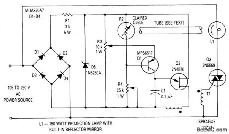
The circuit will regulate the rms output voltage across the load (a projection lamp) to 100 volts 12% for an input voltage between 105 and 250 volts ac. This is accom-plished by indirectly sensing the light output of lamp L1 and applying this feedback signal to the firing circuit (Q1 and Q2) which controls the conduction angle of TRIAC Q3. The lamp voltage is provided by TRIAC Q3, whose conduction angle is set by the firing circuit for unijunction transistor Q2. The circuit is synchronized with the line through the full-wave bridge rectifier. The voltage to the firing circuit is limited by zener diode D5. Phase control of the supply voltage is set by the charging rate of capacitor C1. Q2 will fire when the voltage on C1 reaches approximately 0.65 times the zener voltage. The charging rate of C1 is set by the conduction of Q1, which is controlled by the resistance of photocell R2. Potentiometers R3 and R4 are used to set the lamp voltage to 100 volts when the line voltage is 105 volts and 250 volts, respectively. (View)
View full Circuit Diagram | Comments | Reading(1524)
PAFITY_LINE_INTERCOM
Published:2009/7/1 1:10:00 Author:May
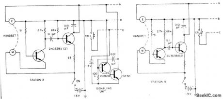
A large number of intercom stations can be tied together. All units are connected in parallel, and the entire system is buzzed by only one signaling circuit. Each unit is powered individually from 1.5-V cells for redundancy. For greater signal volume, 3-V sources can be used for the supplies without changing any other parts of the system. The carbon microphone of a standard telephone handset at each station feeds into a common-base amplifier, and a tandem high-gain common-emitter stage drives the intercom line. All phone earpieces are in parallel across the line. The signaling circuit, also connected across the line, is a simple oscillator that drives all the earpieces. (View)
View full Circuit Diagram | Comments | Reading(762)
INTERCOM
Published:2009/7/1 1:09:00 Author:May

The circuit consists of separate amplifiers-one for each station-rather than a single amplifier and a time sharing arrangement. U1 and U2 are low-voltage audio amplifiers, each of which operates as separate entities with switches at either station controlling which will transmit or receive. With capacitors C7 and C8 included in the circuit, the amplifiers have a gain of 200. Omitting those two components drops the gain to about 20. Other gain levels are available with the addition of a series-connected R/C combination connected between pin 1 and pin 8-for example, a 1000 ohm resistor and 10 μF capaci-tor for a gain of about 150. (View)
View full Circuit Diagram | Comments | Reading(2227)
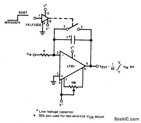
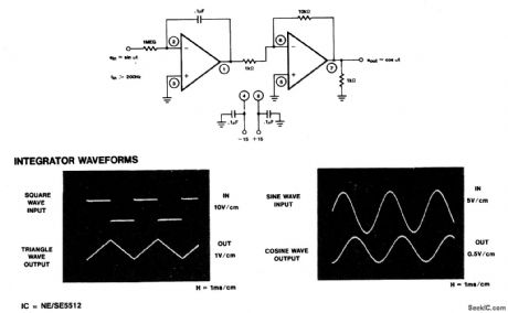
LONG_TIME_INTEGRATOR
Published:2009/7/1 1:07:00 Author:May
View full Circuit Diagram | Comments | Reading(759)
ACTIVE_INTEGRATOR_WITH_INVERTING_BUFFER
Published:2009/7/1 1:07:00 Author:May
View full Circuit Diagram | Comments | Reading(828)
IMPROVED_NON_INVERTING_INTEGRATOR
Published:2009/7/1 1:06:00 Author:May
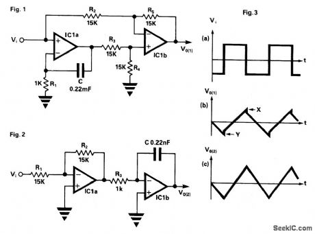
In the circuit in Fig. 1, IC1a produces the integral term required but also has the side effect of producing a proportional term not required, so this term is subtracted by IC1b leaving a pure integral. If the ratio R2/R5 does not exactly match the ratio of R3/R4, the subtraction will not be complete and a small amount of the proportional term will reach the output. The result of this with a squarewave input is shown in Fig. 3a as small steps in the output waveform at points X and Y.This effect can be completely removed by using the simplified circuit shown in Fig.2. Here the signal is pre-inverted by IC1a, then fed to a standard inverting integrator IC1b. The result is a non-inverting integrator with the advantage that the unwanted proportional term is never produced, so it does not need to be subtracted. (View)
View full Circuit Diagram | Comments | Reading(2720)
INSTRUMENTATION_METER_DRIVER
Published:2009/7/1 1:04:00 Author:May
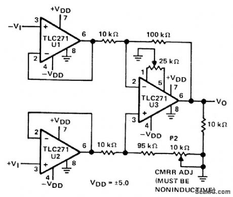
Three op amps U1, U2, and U3 are connected in the basic instrumentation amplifier configuration. Operating from ±5 V, pin 8 of each op amp is connected directly to ground and provides the ac performance desired in this application (high bias mode). P1 is for offset error correction and P2 allows adjustment of the input common mode rejection ratio. The high input impedance allows megohms without loading. The resulting circuit frequency response is 200 kHz at -3 dB and has a slew rate of 4.5 V/μs. (View)
View full Circuit Diagram | Comments | Reading(1591)
INSTRUMENTATION_AMPLIFIER_WITH_±100_VOLT_COMMON_MODE_RANGE
Published:2009/7/1 1:00:00 Author:May
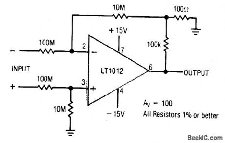
View full Circuit Diagram | Comments | Reading(582)
PULSED_INFRARED_DIODE_EMITTER_DRIVE
Published:2009/7/1 0:57:00 Author:May
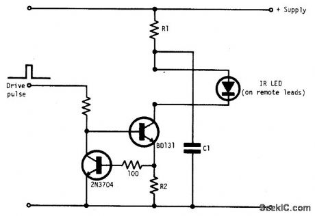
Q1 and Q2 form a constant current drive defmed by R2. (I approximates to the reciprocal of R2 in the circuit shown for values of I greater than 1 amp). The pulse current is drawn from C1 which is recharged during the time between pulses via R1. The value of C1 is determined from the duration and magnitude of the peak current required, and the time constant R1 C1 is determined from the duration between pulses. (View)
View full Circuit Diagram | Comments | Reading(819)
INVISIBLE_INFRARED_PULSED_LASER_RIFLE
Published:2009/7/1 0:55:00 Author:May
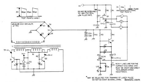
The device generates an adjustable frequency of low to medium powered IR pulses of invisible energy and must be treated with care.The portable battery pack is stepped up to 200 to 300 volts by the inverter circuit consisting of Q1, Q2, and T1. Q1 conducts until saturated, at which time, the base no longer can sustain it in an on state and Q1 turns off, causing the magnetic field in its collector winding to collapse thus producing a voltage or proper phase in the base drive winding that turns on Q2 until saturated, repeating the above sequence of events in an on/off action. The diodes connected at the bases provide a return path for the base drive current. The stepped up squarewave voltage on the secondary of T1 is rectified and integrated on C2. (View)
View full Circuit Diagram | Comments | Reading(648)
LOW_NOISE_INFRARED_DETECTOR
Published:2009/7/1 0:52:00 Author:May

View full Circuit Diagram | Comments | Reading(601)
GAS_ANALYZER
Published:2009/7/1 0:43:00 Author:May
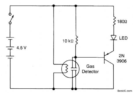
The circuit shows a simple yes/no gas detector. Three 1.5-V D cells are used as a power supply, with S1 acting as an on/off switch. The heater is energized directly from the battery, while the electrodes are in series with a 10 k resistor. The voltage across this resistor is monitored by a pnp transistor. When the sensor is in clean air, the resis-tance between the electrodes is about 40 k, so that only about 0.9 V is dropped across the 10 k resistor. This is insufftcient to turn on the transistor, because of the extra 1.6 V required to forward bias the light emitting diode (LED) in series with the emitter. When the sensor comes in contact with contaminated air, the resistance starts to fall, increasing the voltage dropped across the 10 k resistor. When the sensor resistance falls to about 10 k or less, the transistor starts to turn on, current passes through the LED, causing it to emit. The 180 ohm resistor limits the current through the LED to a safe value. (View)
View full Circuit Diagram | Comments | Reading(927)
RAIN_WARNING_BLEEPER
Published:2009/7/1 0:37:00 Author:May
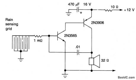
One small spot of rain on the sense pad of this bleeper will start this audio warning.It can also be operated by rising water. The circuit has two transistors, with feedback via capacitor C1, but Trl cannot operate as long as the moisture sense pad is dry. When the pad conducts, Tr1 and Tr2 form an audio oscillatory circuit, the pitch depends somewhat on the resistance. (View)
View full Circuit Diagram | Comments | Reading(792)
ELECTRONIC_ROULETTE
Published:2009/7/1 0:32:00 Author:May
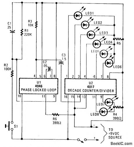
U1 (a 4046 PLL containing a voltage controlled oscillator or VCO, two phase comparators, a source follower, and a Zener diode) is used to produce a low-frequency, pulsed output of about 40 Hz. The VCO's frequency range is determined by R6 and C2, which can. be altered by varying the voltage at pin 9. The rising voltage causes the frequency to rise from zero to threshold and remain at that frequency as long as 51 is closed. When S1 is opened, C1 discharges slowly through RI to ground and the voltage falls toward zero. That produces a decreasing pulse rate. The output of UI at pin 4 is connected to the clock input of U2 (a 4017 decade decoder/driver) at pin 14 via C3. U2 sequentially advances through each of its ten outputs (0 to 9)-pins 1 to 7, and 9 to 11-with each input pulse. As each output goes high, its associated LED is lighted, and extinguished when it returns to the low state. Only eight outputs are used in the circuit, giving two numbers to the spinner of the house. The circuit can be set up so that the LED's lights sequence or you can use some staggered combination; the LEDs grouped in a straight line or a circle. (View)
View full Circuit Diagram | Comments | Reading(1516)
LIGHT_SEEKING_ROBOT
Published:2009/6/30 23:58:00 Author:May

The circuit is light seeking; it will follow a flashlight around a darkened room. A pair of photocells determine the direction in which the robot will move. Each photocell is connected to an op amp configured as a comparator. When sufficient light falls on photocell R2, the voltage at the inverting input (pin 6) of ICl-a will fall below the voltage at the non-inverting input (pin 5), so the output of the comparator will go high, and transistors Q1 and Q2 will turn on. That will enable relays RY1 and RY2, and thereby provide power for the right motor. The robot will then turn left. Likewise, when light falling on R3 lowers its resistance, Q2 and Q3 will turn on, the left motor will energize, and the robot will turn right. (View)
View full Circuit Diagram | Comments | Reading(3043)
TWILIGHT_TRIGGERED_CIRCUIT
Published:2009/6/30 23:53:00 Author:May
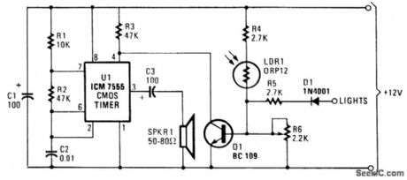
As dusk begins to fall, the sensor (a cadmium-sulftde light-dependent resistor or LDR) operates a small horn to provide an audible reminder that it's time to turn on your lights. To turn the circuit off-simply turn your headlights on and the noise stops. The base of Q1 is fed through a voltage divider formed by R4, LDRl-a light-dependent resistor with an internal resistor of about 100 ohms under bright-light conditions and about 10 megohms in total darkness-potentiometer R6. Q1's base voltage depends on the light level received by LDR1 and the setting of R6. If LDR1 detects a high light level, its resistance decreases, thereby providing a greater base current for Q1, causing it to conduct. When Q1 conducts, pin 4 of UI is pulled to near ground potential, muting the oscillator. If; on the other hand, LDR1 detects a low light level, its resistance increases (reducing base currentto Q1), cutting off the transistor and enabling the oscillator. In actual practice, you set R6 so that at a suitable light level (dusk), the oscillator will sound.The anode of diode Dl connects to the light switch, where it connects to the vehicle's parking lights. With the lights switched off, that point is connected to the negative chassis by way of the parking lamp. That has no effect on the circuit, as Dl blocks any current flow to ground from Q1's base via R6 and the sidelight lamps. When the lights are switched on, the anode of Dl is connected to the positive supply via the parking lamp switch, thereby applying a voltage to the base of Q1, biasing it into conduction. With Q1 conducting, pin 4 of UI is pulled virtually to ground, disabling the oscillator even though LDRl's resistance is not enough to do so. (View)
View full Circuit Diagram | Comments | Reading(1069)
Digital_power_monitor_with_early_warning
Published:2009/7/24 12:21:00 Author:Jessie
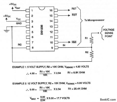
This circuit shows a DS1236 that is used to control a digital-system power supply. The DS1236 generates a nonmaskable interrupt (NMI ) for early warning of power failure to a microprocessor. A precision comparator monitors the voltage level at the In pin, relative to an internal reference. The In pin is a high-impedance input that allows for a user-defined sense point. An external resistor voltage divider interfaces with voltage signals. The sense point can be taken from the 5-V supply or from a higher voltage level that is closer to the main system power input. Because the In trip point VTP is 2.54 V,the proper values for R1 and R2 can be determined by the equations. Dallas Semiconductors, Product Data Book, 1992/1993, p. 7-74. (View)
View full Circuit Diagram | Comments | Reading(644)
Digital_signal_processing_system_with_anti_aliasing
Published:2009/7/24 10:46:00 Author:Jessie

In this circuit, a MAX274 provides a front-end 10-kHz low-pass filter to a digital signal-processing (DSP) system. Signals between dc and 10 kHz are digitized by a 12-bit sampling MAX167 A/D. The DSP processor receives samples at a rate of 48 kHz. The input signal is filtered by a MAX274 that is configured as a 10-kHz 8th-order Butterworth low-pass filter. Signals above 24 kHz (the Nyquist frequency) are attenuated 60 dB. Additional rolloff in the incoming signal reduces potential alias frequencies below the theoretical 74-dB noise floor of the 12-bit system. Maxim, 1992, Applications and Product Highlights, p. 7-4. (View)
View full Circuit Diagram | Comments | Reading(1240)
Flash_EPROM_programmer_plus_adjustable_LCD_supply
Published:2009/7/24 10:43:00 Author:Jessie
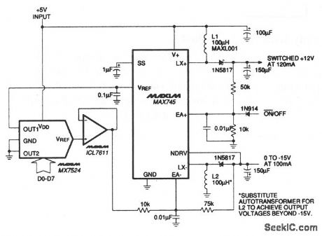
The MAX745 generates both positive and negative boosted outputs from a +5-V supply. This circuit is configured for small microprocessor systems, and contains a DAC to adjust the negative voltage for LCD contrast control. The circuit also provides for switching on and off the + 12-V output to program flash EPROMs. Maxim, 1992, Applications and Product Highlights, p. 4-9. (View)
View full Circuit Diagram | Comments | Reading(1049)
| Pages:306/471 At 20301302303304305306307308309310311312313314315316317318319320Under 20 |
Circuit Categories
power supply circuit
Amplifier Circuit
Basic Circuit
LED and Light Circuit
Sensor Circuit
Signal Processing
Electrical Equipment Circuit
Control Circuit
Remote Control Circuit
A/D-D/A Converter Circuit
Audio Circuit
Measuring and Test Circuit
Communication Circuit
Computer-Related Circuit
555 Circuit
Automotive Circuit
Repairing Circuit