
Basic Circuit
Index 308
AGC_WITH_FET
Published:2009/6/30 22:25:00 Author:May
FET serves as nonlinear element in fastacting instrumentation circuit han-dling wide range of signals. R1 and R2 attenuate input signal so FET input is less than 25 mV for inputs up to 2 VRMS. Article covers design and performance. Gain is almost linear with gate voltage of FET,-R D Pogge,Designers'Guide to:Basic AGC Amplifier Design、EDNMagazine,Jan,20、1974、p 72-76 (View)
View full Circuit Diagram | Comments | Reading(1182)
AGC_LOOP_FOR_MOSFETS
Published:2009/6/30 22:22:00 Author:May
Used at output of 9-MHz IF amplifier in commercial receiver to divide desired control-voltage magnitude and swing for FT0601 MOSFETS in IF strip. MOSFETs are biased by 2.1,V zeners in source leads in FETs, to drive gate-2 voltage sufficiently nega-tive for full AGC action.-G. Ricaud, Modifying the W1CER/W1FB AGC Loop for Usewith M0S-FET I-F Amplifiers, OST, June 1977, p 47 (View)
View full Circuit Diagram | Comments | Reading(2330)
CONTROL_WITH_EXTERNAL_DIODE
Published:2009/6/30 22:21:00 Author:May
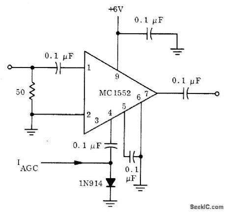
External resistances normally used with Motorola MC1552 video amplifier are replaced by 1N914 or equivalent diode so gain of amplifier is de-termined by AGO current through diode. Arrangement gives wide range of gain control, but lowest obtainable level of gain is normal unmodified gain off amplifier. Same circuit can be used with MC1553 highgain video amplifier.- A Wide Band Monolithic Video Amplifier, Motorola, Phoenix, M, 1973, AN-404 p 10. (View)
View full Circuit Diagram | Comments | Reading(645)
TTL_driver
Published:2009/7/24 9:35:00 Author:Jessie

This circuit uses a 339 comparator as a TTL driver. Raytheon Linear Integrated Circuits, 1989, p. 5-30. (View)
View full Circuit Diagram | Comments | Reading(900)
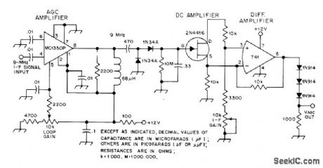
30_MHz_AGO_LOOP
Published:2009/6/30 22:20:00 Author:May
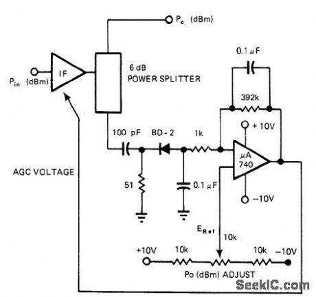
Low-pass filter serves as loop giving dosed-loop bandwidth of at least 5 kHz. Loop operates in square-law region of de-tector diode. Inputs to IF amplifier are in range from -60 dBm to -to dBm, and AGC action provides 30-MHz IF output of -15 dBm. Power splitter ensures that detector also operates at -15 dBm. Article gives design equations and performance curves.-R. S. Hughes, Design Au-tomatic Gain Control Loops the Easy Way. EDN Magazine, Oct, 5, 1978, p 123.128. (View)
View full Circuit Diagram | Comments | Reading(614)
LOW_PHASE_SHIFT
Published:2009/6/30 22:19:00 Author:May
Voltage-control led amplifier has less than 3°phase shift over gaincontrol range of 40 dB at frequencies up to 10 MHz, as required for AGO circuits. Current generator Q2 controls gain of wideband resistance-coupled amplifier Q1. Gain of al increases lineady with amplitude of positive control voltage on base of Q2.-A. H. Hargrove, Simple Circuits Control Phase-Shift, EDNMagazine, Jan, 1, 1971, p 39. (View)
View full Circuit Diagram | Comments | Reading(864)
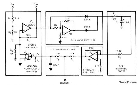
TWO_DECADE_RANGE
Published:2009/6/30 22:17:00 Author:May
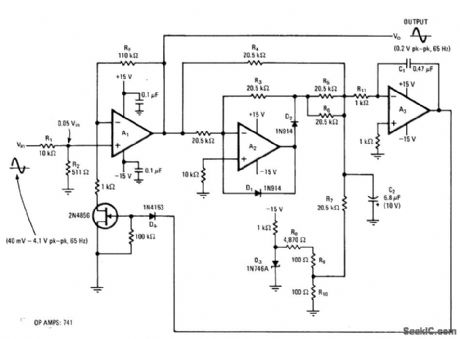
Output is maintained at 0.2V for inputs from 40mV to 4.1V. Voltage controlled JFET serves as variable control element. Comparator A3 produces error voltage that determines gain of A1, A2, and diodes form full-wave rectifier. Developed for use in radar seeker device to prevent overload of amplifier as target gets closer.-C. Marco, Automatic Gain Control oporates over Two Decades,Eleetriics, Aug,16、1973 p 99-100;reprinted in″Circuits for Electronics Engineers,″Electronics 1977、p 44-46 (View)
View full Circuit Diagram | Comments | Reading(677)
FET_GlVES_30_dB_GAIN_RANGE
Published:2009/6/30 22:16:00 Author:May
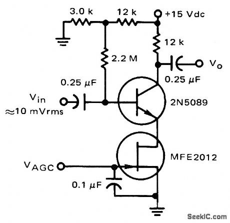
Only 1-V change in gate-source voltage of FET changes voltage gain over full range. Possible drawback is harmonic distortion due to unbypassed emit-ter degeneration.- Low Frequency Applica-tions of Field-Effect Transistors. Mototola, Phoenix, AZ, 1976, AN-511A, p 8. (View)
View full Circuit Diagram | Comments | Reading(597)
HANG_AGC
Published:2009/6/30 22:16:00 Author:May
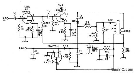
Provides very fast attack time with no AGC pop. Diodesare 1N914. When voltage across R10-08 decays below that across R9-C7, 03 conducts and clamps AGO bus to ground.AGO threshold is determined by value of RT, between 100K and 470K. AGC line must have high impedance, as with FET IF system. With l0 or bipolar IF amplifier, use low-impedance driver.T1 is audio transformer with 10K primary and 2K secondary (Radio Shack 273-1378).-D. Ste-vens, Solid-State Hang AGC, QST, July 1975, p 44. (View)
View full Circuit Diagram | Comments | Reading(1355)
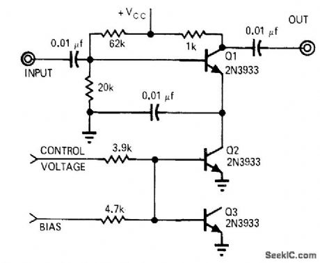
AGC_WITH_CMOS_LOGIC
Published:2009/6/30 22:14:00 Author:May
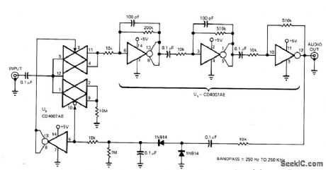
First stage U2, using CD4007AE, is wired as two-line demultiplexer with only one output acting as transmission gate. Gain is lower in first stage to reduce noise. U1 is used as three-stage high-gain audio amplifier in which first two stages have low-pass filtering for stability. AGO voltage, developed from audio output, is fed back to U, to turn transmission gate off when gain must be reduced. Audio output is about 2.5 V P-P for inputs of 2 mV and greater.-K. H. Fleischer, Tum Dig-ital CMOS IC's into a Low-Level AGC Amplifier, EDNMagazine, Oct.5,1977, p 99. (View)
View full Circuit Diagram | Comments | Reading(844)
ECL_TTL_to_TTL_translator
Published:2009/7/24 9:34:00 Author:Jessie
This circuit adapts either ECL Or TTL circuits using an RC4508 comparator. Raytheon Linear Integrated Circuits, 1989, p. 5-14. (View)
View full Circuit Diagram | Comments | Reading(810)
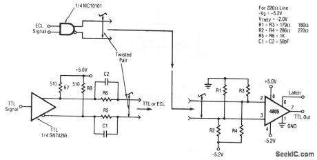
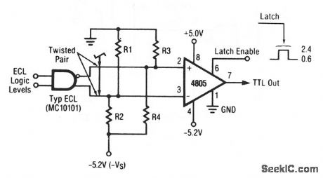
ECL_to_TTL_translator_tracking
Published:2009/7/24 9:32:00 Author:Jessie
This circuit uses an RC4508 comparator as an ECL-(single-ended) to-TTL translator with tracking ECL reference. Raytheon Linear Integrated Circuits, 1989, p. 5-13. (View)
View full Circuit Diagram | Comments | Reading(848)
MEASURING_AF_DISTORTION
Published:2009/6/30 22:08:00 Author:May
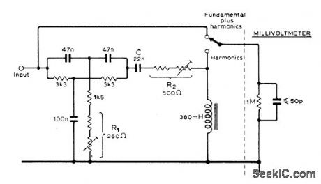
Passive highpass 1-kHz filter is used with audio millivoltmeter to improve accuracy of distortion measurements for low-impedance sources at 1 kHz.Filter removes low-frequency noise from input signal and compensates for loss of harmonic frequency. Applications include setting bias and recording levels of tape recorder. Adjust R1 for best null, then ad just R2 and value of C to equalize responses at harmonics.-J. B. Cole, Passive Network to Measure Distortion, Wireless World, Jan. 1978 p 60.
(View)
View full Circuit Diagram | Comments | Reading(672)
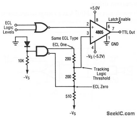
ECL_to_TTL_translator
Published:2009/7/24 9:26:00 Author:Jessie
This circuit uses an RC4508 comparator as an ECL-to-TTL translator. Raytheon Linear Integrated Circuits, 1989, p. 5-12. (View)
View full Circuit Diagram | Comments | Reading(1146)
RTL_or_high_current_driver
Published:2009/7/24 9:24:00 Author:Jessie
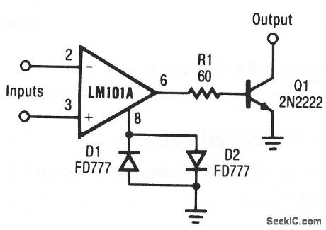
This circuit uses an LM101A as a voltage comparator to drive RTL or other high-current devices. Raytheon Linear Integrated Circuits, 1989, p. 4-247. (View)
View full Circuit Diagram | Comments | Reading(753)
Basic_digital_D_A_converter
Published:2009/7/24 9:22:00 Author:Jessie
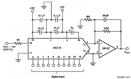
This circuit shows the classic DAC/op-amp combination that produces a digital D/A converter. VOUT is selected, in steps, by the binary signals at the digital input of DAC-10, with the highest VOUT set by VREF at pin 16. VREF is supplied by REF-01 (Fig.4-1). With the circuit assembled using the values shown (0.01 μF is typical for CC), apply binary inputs (typically -VS to -VS plus 36 V) at pins 5 through 14, stating with all zeros (or all 1s). Notice that VOUT varies (in steps) between 0 and a typical 9.9 V. Record actual values. Raytheon Linear Integrated Circuits, 1989, p. 495. (View)
View full Circuit Diagram | Comments | Reading(1090)
POSITIVE_INPUT_V_F_
Published:2009/6/30 21:28:00 Author:May
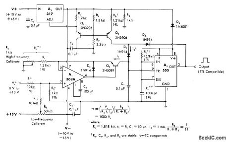
Input voltages from 0 to 10 V are divided by R1 and R2 for application to noninverting input of current source A1. 555 timer A2 provides functions of precision mono MVBR and level sensor.Regulator A3 acts as gated current source and provides stabilized voltage output for 555 and 308A.—W.G.Jung, IC Timer Cookbook, Howard W.Sams, Indianapolis, IN, 1977, p 184-192. (View)
View full Circuit Diagram | Comments | Reading(598)
LEDs_DISPLAY_VU_PEAKS
Published:2009/6/30 21:27:00 Author:May
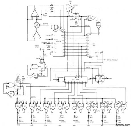
Exponential coding of Precision Monolithics DAC-76 D/A converter is used to good advantage in peak-reading VU indicator with logarithmic weighting, driving LED display, Input audio is converted by DAC-76,CMP-01 comparator,and 2502 successiveapproximation A/D converter after being sampled by sample-and-bold input circuit,A/D converter is clocked at 500kHz and completes conversion every 18μs,which is fast enough to track audio signals ,4 most significant magnitude bits drive 3205 1-of-8 decoder which is enabled by most significant bit,Resulting eight output levels,separated by 3-dB increments, drive 8-bit RS LATCH USING 74279 chips,updated every 25 ms hy 40-Hz display multiplex clock,-W.Jung and W.Ritmanich, Audio applicateions tof the DAC-76 Companding D/A Converter, Precision Monolithics,Santa Clara,CA 1977,AN-28, p 6 (View)
View full Circuit Diagram | Comments | Reading(693)
BIPOLAR_OUTPUT
Published:2009/6/30 21:24:00 Author:May


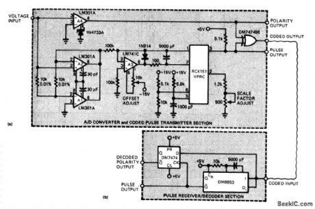
Low-cost voltage-to-fre-quency converter IC is here used in A/D converter circuit that will accept bipolar inputs and generate positive-going pulses to indicate positive input voltages and negative-going pulses for negative input voltages. Opamps A1 and A2 form negative-output absolute-value circuit that feeds opamp A3 and RC4151 voltage-to-frequency converter, for generating 10-μs negative-going pulses with repetition-rate scale factor of 1 kHz/V. Full-scale input is 20 V P-P.Opamp A4 is ground-referenced voltage comparator having zener clamp, providing TTL-compatible logic output for indicating input polarity. Pulse-receiver/decoder section takes digitally coded signals arriving from transmitter, for processing by data line or D flip-flop and two trigger inputs of dual-edge retriggerable mono MVBR This generates 25-μs negative-going output pulse for each 10-μs input pulse from data line. Logic 1 on complementary output of flip-flop indicates that original input voltage to transmitter was positive.—E. J.DeWath, Low-Cost A/D Converter Transmits and Receives, EDN Magazine, Jan. 5, 1977, p 35. (View)
View full Circuit Diagram | Comments | Reading(1187)
Digital_power_monitor_with_watchdog_timer_and_pushbutton
Published:2009/7/24 12:20:00 Author:Jessie
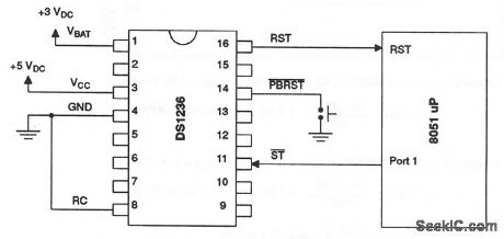
This circuit shows a DS1236 that is used to monitor and control the power-supply and software execution of a processor-based system, and to provide a pushbutton reset. When an out-of-tolerance condition occurs (when VCC is below 4.5 V for 10% operation, or below 4.75 V for 5% operation), the RST and RST outputs are driven to the active state. On power-up, RST and RST are held active for a minimum of 25 ms (100 ms typical) after 4.5 V (or 4.75 V) is reached to allow the power supply and processor to stabilize. The pushbutton input PBRST is debounced and timed so that reset signals are driven to the active state for 25 ms minimum. The watchdog-timer function forces RST and RST to the active state (shutting down the processor) when the ST input is not stimulated for a predetermined time period (because of some failure in software execution). The watchdog time period is 400-ms typical (600-ms maximum). The ST input can be taken from address, data, and/or control signals. When the processing is executing software, these signals are present, and cause the watchdog to be reset prior to time-out. Dallas Semiconductors, Product Data Book, 1992/1993, p. 10-73. (View)
View full Circuit Diagram | Comments | Reading(715)
| Pages:308/471 At 20301302303304305306307308309310311312313314315316317318319320Under 20 |
Circuit Categories
power supply circuit
Amplifier Circuit
Basic Circuit
LED and Light Circuit
Sensor Circuit
Signal Processing
Electrical Equipment Circuit
Control Circuit
Remote Control Circuit
A/D-D/A Converter Circuit
Audio Circuit
Measuring and Test Circuit
Communication Circuit
Computer-Related Circuit
555 Circuit
Automotive Circuit
Repairing Circuit