
Index 293
SCR circuit using TCA780 and transistor amplification 59
Published:2011/4/17 21:08:00 Author:Nicole | Keyword: SCR, transistor
The SCR output current can reach 30A. Adopting potentiometer Rp1 can adjust output DC power. Because the integrated trigger TCA780 only has about 50mA output current, the SCR needs 1A control current, so it should connect a amplifier circuit composed of NPN tube. (View)
View full Circuit Diagram | Comments | Reading(818)
NE555 alarm circuit diagram
Published:2011/4/17 20:36:00 Author:Ecco | Keyword: alarm circuit
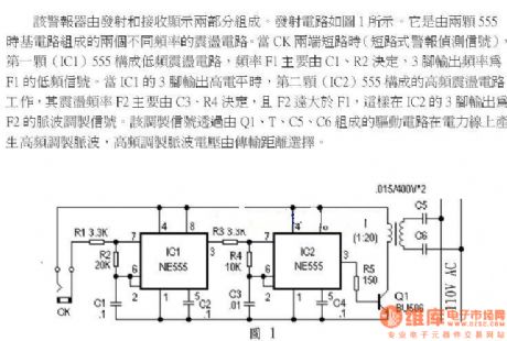
The alarm is composed of two parts of the transmitting and receiving. Transmitting circuit is shown in Figure 1. It consists of two vibration temperature circuits with different frequencies and they are composed of two 555 time-base circuits. When the two ends of CK are in short circuit, the first(IC1) 555 constitutes a low-frequency shock temperature circuit, the frequency F1 is mainly decided by C1, R2, the output frequency of pin 3 is the low-frequency signal of F1. When the output of pin 3 is in high level, the second (IC2) 555 constitutes a high-frequency shock temperature circuit, the frequency F2 is mainly decided by C3, R4, and F2 much higher than F1, so the output of pin 3 is the pulse modulated signal of F2. The modulation signal throughs the driving circuit composing of Q1, T1, C5, C6 and produces high frequency modulation pulse on the power line, the voltage of high frequency modulation pulse is decided by transmission distance.
(View)
View full Circuit Diagram | Comments | Reading(1307)
Simulation voltage limit device principle circuit
Published:2011/4/15 2:13:00 Author:Jessie | Keyword: Simulation voltage limit device, principle
View full Circuit Diagram | Comments | Reading(554)
6N16B Tube feet definition pins definition circuit
Published:2011/4/15 2:30:00 Author:Jessie | Keyword: Tube feet, definition, pins
View full Circuit Diagram | Comments | Reading(720)
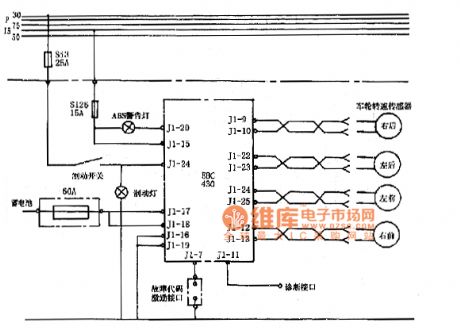
Hongqi ant-ilock braking system ABS circuit
Published:2011/4/15 2:31:00 Author:Jessie | Keyword: ant-ilock braking system, ABS
View full Circuit Diagram | Comments | Reading(541)
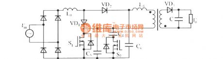
Full-bridge single stage PFC converter
Published:2011/4/15 2:18:00 Author:Nicole | Keyword: single stage PFC, converter
View full Circuit Diagram | Comments | Reading(567)
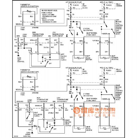
Buick seat heater circuit
Published:2011/4/14 20:36:00 Author:Jessie | Keyword: seat heater
View full Circuit Diagram | Comments | Reading(742)
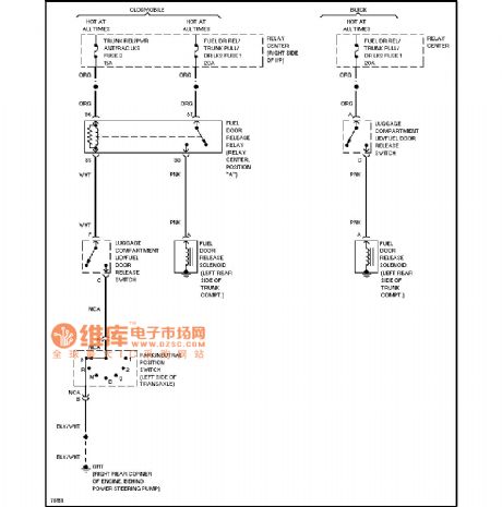
Buick throttle circuit
Published:2011/4/14 20:37:00 Author:Jessie | Keyword: throttle
View full Circuit Diagram | Comments | Reading(473)
The alarm circuit diagram of miner light
Published:2011/4/14 21:13:00 Author:Ecco | Keyword: alarm circuit , miner light
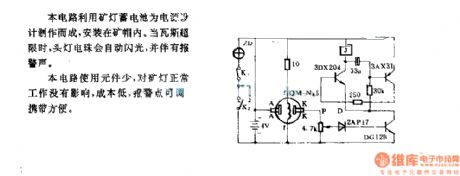
In the circuit, the batteries of miner's lamp is used as power supply and installed in the mine cap. When the gas is over the limit, the light bulb will automatically flash with the alarm. This circuit uses few components, it has no impact on the miner's work, it has the advantages of low cost, adjustable alarm points, easy to carry. (View)
View full Circuit Diagram | Comments | Reading(655)
The alarm circuit diagram for safety box and other metal objects
Published:2011/4/14 21:25:00 Author:Ecco | Keyword: alarm circuit , safety box , metal objects
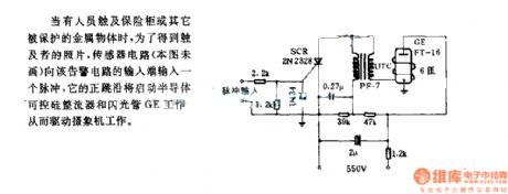
When someone touches the safety box or other protected metal objects, in order to get the photo of the toucher, the sensor circuit inputs a pulse to the alarm circuit, and its positive edge will start the semiconductor and thyristor flash GE, then driving the camera work.
(View)
View full Circuit Diagram | Comments | Reading(1096)
Light control alarm circuit diagram
Published:2011/4/14 21:01:00 Author:Ecco | Keyword: Light control, alarm circuit
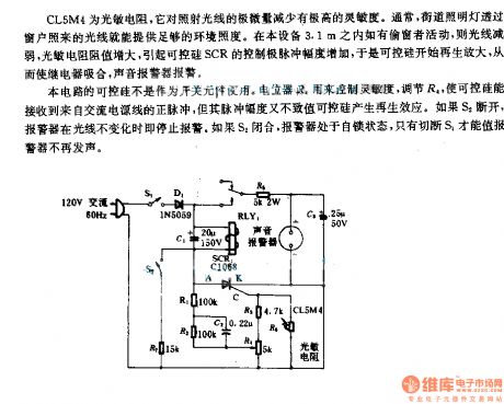
As a photoresistor, CL5M4 has a high sensitivity to the reducing of light exposure. Usually, the light from the street lights can provide enough ambient illumination. If there was an activity to steal the window in 3.1m of the device, the light would be weakened, the resistance of photosensitive resistor and SCR controlling pulse amplitude would increase. Then the SCR starts regenerative amplification, the relay pulls in, the sound alarm warns.
The SCR in the circuit is not used as a switching element. Potentiometer R4 is used to control sensitivity, adjust the R4, to make SCR receive the positive pulse from the AC power, but the pulse amplitude could not make the SCR produce renewable effects. If S2 turns off, the alarm will stop the warning when the light will not change any more. If S2 is closed, the alarm is in self-locking state, the alarm stops warning by cuting off S1.
(View)
View full Circuit Diagram | Comments | Reading(764)
Back up supply control circuit
Published:2011/3/31 21:21:00 Author:may | Keyword: Back up supply control
View full Circuit Diagram | Comments | Reading(483)
Photoelectric control circuit used in cotton feeder control
Published:2011/4/14 2:04:00 Author:Nicole | Keyword: photoelectric control, cotton machine control
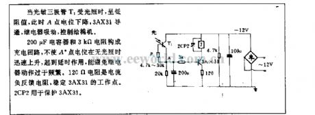
When phototransistor T1 has illumination, it is low resistivity, then the potential in A point is falling, 3AX31 is conduction, relay is pull-in, to control the cotton feeder.
200μF capacitor and 3kΩ resistance form charge loop, to prevent the potential in A point from rising, it is a delay function, it can avoid too much actions of relay. 120Ω resistance is current negative feedback resistance, it is used to steady the work point of 3AX31. 2CP2 is used to protect 3AX31. (View)
View full Circuit Diagram | Comments | Reading(490)
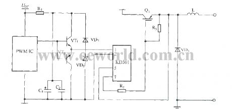
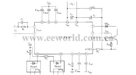
TX-KD501 application wiring diagram driver
Published:2011/4/14 3:59:00 Author:Nicole | Keyword: wiring diagram, driver
View full Circuit Diagram | Comments | Reading(531)
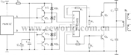
TX-KAl01 IGBT driver application wiring diagram
Published:2011/4/14 4:04:00 Author:Nicole | Keyword: IGBT driver
View full Circuit Diagram | Comments | Reading(1023)
TX-KD301 application wiring diagram driver
Published:2011/4/14 4:14:00 Author:Nicole | Keyword: driver
View full Circuit Diagram | Comments | Reading(578)
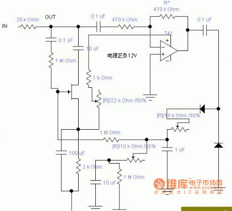
Operational amplifier instrument circuit
Published:2011/4/13 22:55:00 Author:Jessie | Keyword: Operational amplifier, instrument
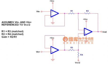
The circuit's gain is veryeasy tocalculate. But this circuit also has a weakness: that is in the circuit, the two resistances must be replaced together, and they must be equivalent. Another weakness is, the first level op-amp dose not produce any useful gain. (View)
View full Circuit Diagram | Comments | Reading(647)
Square wave and triangle wave oscillating circuit
Published:2011/4/14 1:52:00 Author:Jessie | Keyword: Square wave, triangle wave, oscillating

View full Circuit Diagram | Comments | Reading(499)
NE5534 hi-fi telephone power amplifier circuit diagram
Published:2011/4/14 3:03:00 Author:Jessie | Keyword: telephone, power amplifier
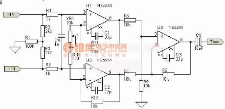
View full Circuit Diagram | Comments | Reading(6264)
Linear DC voltage multiplier circuit
Published:2011/4/14 2:15:00 Author:Jessie | Keyword: Linear, DC voltage, multiplier
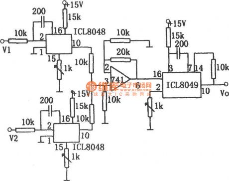
This circuit has two ICL8048 logarithmic amplifiers, ananti-logarithmic amplifier ICL8049, anda 741 op-amp. The relationship between output voltage andtwo input voltages is: Vo=V1V2/10. V1 and V2are +0.1 ~ +10VDC voltage. When the output voltageis +10V, its accuracyis 1%. (View)
View full Circuit Diagram | Comments | Reading(1233)
| Pages:293/312 At 20281282283284285286287288289290291292293294295296297298299300Under 20 |
Circuit Categories
power supply circuit
Amplifier Circuit
Basic Circuit
LED and Light Circuit
Sensor Circuit
Signal Processing
Electrical Equipment Circuit
Control Circuit
Remote Control Circuit
A/D-D/A Converter Circuit
Audio Circuit
Measuring and Test Circuit
Communication Circuit
Computer-Related Circuit
555 Circuit
Automotive Circuit
Repairing Circuit