
Circuit Diagram
Index 1884
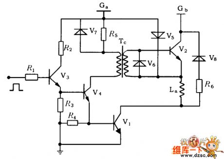
Stepping motor drive circuit diagram
Published:2011/5/12 20:54:00 Author:Nicole | Keyword: Stepping motor drive
View full Circuit Diagram | Comments | Reading(537)
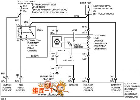
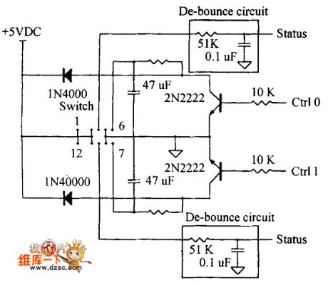
Cadillac deville cruise control circuit diagram
Published:2011/5/12 21:03:00 Author:Nicole | Keyword: Cadillac deville, cruise control
View full Circuit Diagram | Comments | Reading(1170)
F107 series dual power universal single op amp circuit diagram
Published:2011/5/12 4:42:00 Author:Rebekka | Keyword: universal single op amp circuit, dual power
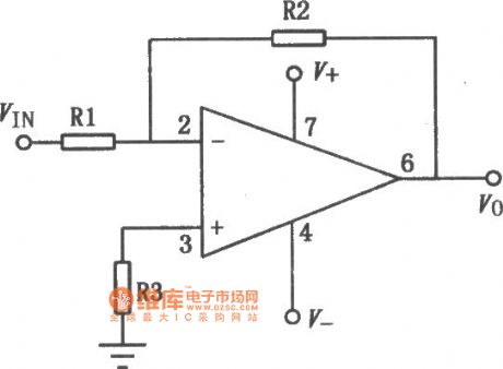
F107 series operational amplifier is single general-purpose internal compensated op amp. Its input current is small. It does not need external compensation components. It is suitable for the integrator, sample maintain and low-frequency waveform generator. The similar or directly substitution models are F107MT, F207LT, F307CT, F107MD, F207LD, F307CD, Fl07MJ, F207LJ, F307CJ, F307CP, SM107, SG207, SG307, LMl07, LM207, LM307 and so on. The typical application circuit is shown as above. (View)
View full Circuit Diagram | Comments | Reading(828)
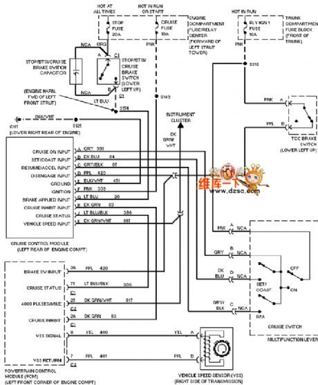
Cadillac deville electronic suspension circuit diagram
Published:2011/5/12 21:00:00 Author:Nicole | Keyword: Cadillac deville, electronic suspension
View full Circuit Diagram | Comments | Reading(626)
Optical switch drive circuit diagram
Published:2011/5/12 20:59:00 Author:Nicole | Keyword: Optical switch drive
View full Circuit Diagram | Comments | Reading(776)
Bootstrap IR2110 integrated drive circuit diagram
Published:2011/5/12 20:45:00 Author:Nicole | Keyword: Bootstrap, integrated drive
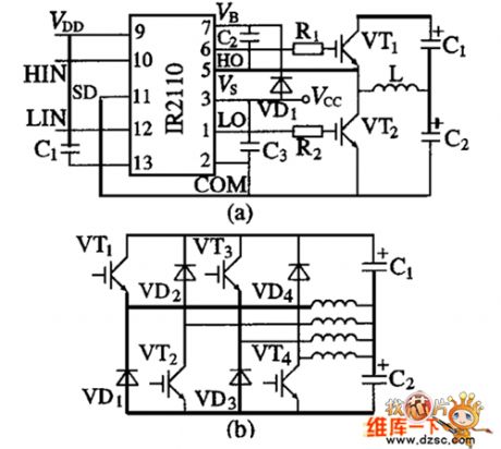
View full Circuit Diagram | Comments | Reading(1835)
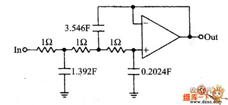
LC filter circuit diagram
Published:2011/5/12 20:44:00 Author:Nicole | Keyword: filter, LC
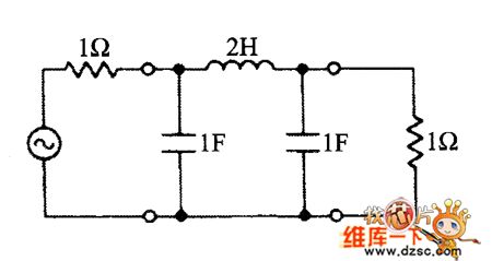
View full Circuit Diagram | Comments | Reading(1618)
Delay circuit with fixed-frequency coefficients
Published:2011/5/12 5:52:00 Author:Rebekka | Keyword: Delay circuit , fixed-frequency coefficients
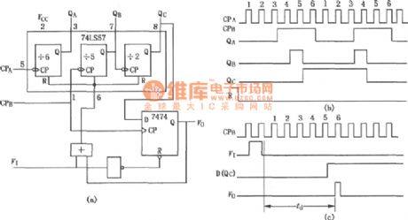
Figure is Delay circuit with fixed-frequency coefficients. The circuit is composed of the 60 divider and D flip-flop 7474. 74LS57 has a 10 frequency divider that composed of an independent 6 divider, a 5 frequency and a 2 frequency level. Its output ends are QA, QB and QC. (View)
View full Circuit Diagram | Comments | Reading(2015)
BA6392FP-the servo-driven intergrated circuit
Published:2011/5/12 20:53:00 Author:Borg | Keyword: servo-driven, intergrated circuit
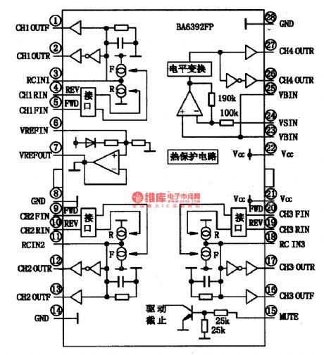
BA6392FP is a single door integrated circuit which is servo-driven by laser heads, and it is widely used in VCD and SVCD of home and abroad.1.The internal circuit BA6392 contains 4-channel BTL drive circuit, which can receive the PWM control signals output by digital servo integrated circuits, then, after filtering and amplifying them, it will drive the focus and tracking coils , feed and spindle motors of laser heads servo parts. The internal circuit of the chips is shown in Figure 1.
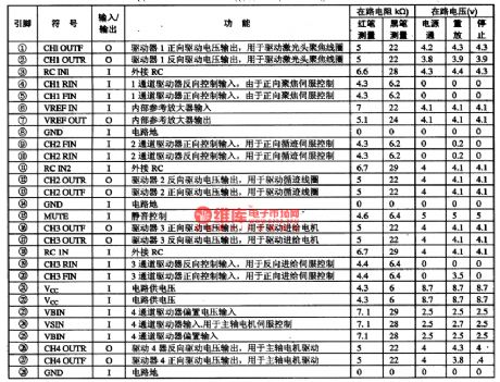
2.Pin functions and data BA6392FP is in 28-pin dual in-line package.
(View)
View full Circuit Diagram | Comments | Reading(1600)
300W high-fidelity power amplifier circuit diagram
Published:2011/5/12 2:07:00 Author:Rebekka | Keyword: 300W high-fidelity power amplifier
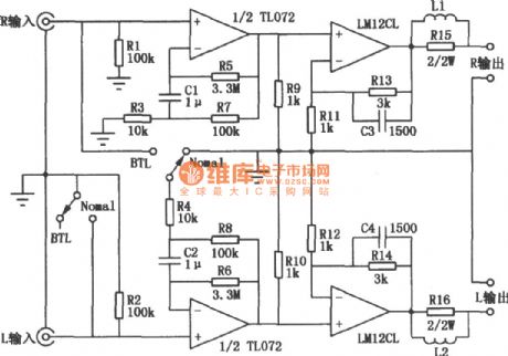
The output power of the amplifier circuit is 300W when it is 8Ω load and BTL mono; When it is load 6Ω and the stereo outputs, the power is l00W + 100W. The circuit uses high-power amplifier LM21CL produced by National Semiconductor. It uses ordinary metal TO-3 package (size and general, like high-power transistor), the rated output power is 150W, the maximum supply voltage is 80V, the maximum output current is 10A, the circuit is shown as above. (View)
View full Circuit Diagram | Comments | Reading(3692)
5A regulated power supply circuit diagram composed of LM340T integrated regulator
Published:2011/5/12 20:45:00 Author:Ecco | Keyword: 5A , regulated power supply , integrated regulator
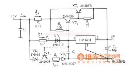
5A regulated power supply circuit diagram(providing power for TTL IC)composed of LM340T integrated regulator
(View)
View full Circuit Diagram | Comments | Reading(1321)
3A regulated power supply circuit diagram composed of LM5000 integrated regulator
Published:2011/5/12 20:46:00 Author:Ecco | Keyword: 3A , regulated power supply , integrated regulator
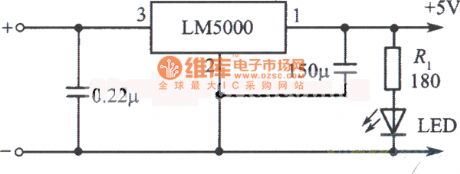
3A regulated power supply circuit diagram(providing power for TTL IC)composed of LM5000 integrated regulator
(View)
View full Circuit Diagram | Comments | Reading(548)
Long time delay timer controller (CD4060, CD4518, CD4069) circuit diagram
Published:2011/5/12 6:16:00 Author:Rebekka | Keyword: Long time delay timer controller
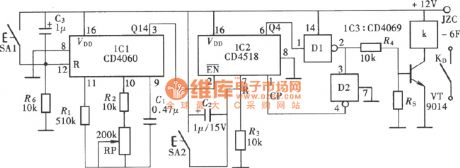
Long time delay timer controller (CD4060, CD4518, CD4069) circuit composed of CD4060, CD4518 andCD4069.
It is a time base circuit composed of a CD4060. The timing time base pulse generated by the circuit passes the internal divider and outputs time base signal. And then passes the peripheral frequency divider circuit to obtain the required timing control time. (View)
View full Circuit Diagram | Comments | Reading(4393)
Low-noise instrumentation amplifier circuit composed of OPA37
Published:2011/5/12 6:21:00 Author:Rebekka | Keyword: Low-noise instrumentation amplifier

Low-noise instrumentation amplifier circuit composed of OPA37 is shown as above. This circuit uses a low noise precision op amp as a pre-OPA37 differential input stage. And it uses precision unity gain amplifier INA105 as the output level.
The overall gain of the circuit is Av = (1 +2 RF/R3) × 1 = 1 +2 × 5/0.1 = 100 times. The offset voltage is about 10/μV. The common mode rejection ratio is about 106dB. The bandwidth is about 500kHz. (View)
View full Circuit Diagram | Comments | Reading(773)
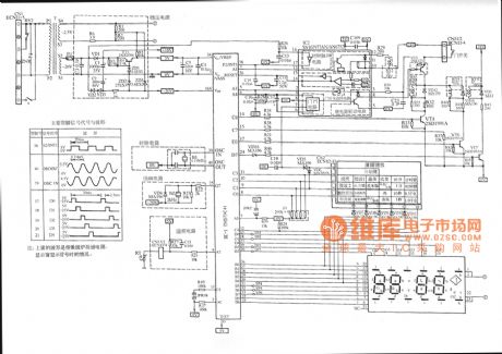
Panasonic NN-K652 computerized microwave circuit diagram
Published:2011/5/12 20:52:00 Author:Ecco | Keyword: Panasonic , computerized microwave
View full Circuit Diagram | Comments | Reading(2246)
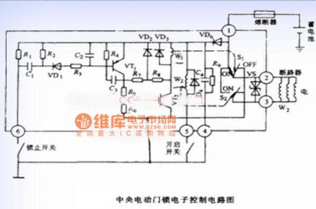
The central power door locks electronic control circuit diagram of Santana 2000
Published:2011/5/12 20:48:00 Author:Ecco | Keyword: central , power door locks , electronic control, Santana 2000
View full Circuit Diagram | Comments | Reading(615)
Electronic temperature sensor circuit with the 4-bit horizontal-vertical converter
Published:2011/5/12 20:47:00 Author:TaoXi | Keyword: Electronic temperature sensor, 4-bit, horizontal-vertical converter
Electronic temperature sensor circuit with the 4-bit horizontal-vertical converter (View)
View full Circuit Diagram | Comments | Reading(749)
LC active filter circuit diagram
Published:2011/5/12 20:43:00 Author:Nicole | Keyword: active filter, LC
View full Circuit Diagram | Comments | Reading(1166)
Digital telemetering thermometers FDD5 and JDD5
Published:2011/5/11 19:30:00 Author:TaoXi | Keyword: Digital telemetering thermometer
Transmitter circuit:
The temperature detecting circuit is composed of the temperature integrated sensor AD590, this circuit changes the temperature variation into the output current variation. AD590's output current is proportional to the measurement temperature, as the temperature increases, the output current increases with the 1μA/K constant ratio. When the output current gets through RP2, at the top of RP2 forms the voltage, and this voltage is amplified by the voltage amplifier and is used as the voltage-frequency changer's control voltage.
Receiving circuit: (View)
View full Circuit Diagram | Comments | Reading(680)
Positive and negative pulse delay circuit compoed of CD4013
Published:2011/5/12 6:33:00 Author:Rebekka | Keyword: Positive and negative pulse delay
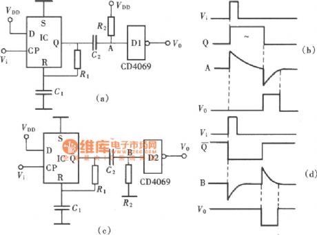
In the digital circuits and automatic control circuit, sometimes you need to delay the inputed pulse signal for a while and then output the signal. This can accommodate the needs of post-level control circuit. One of the application scheme is to use the pulse delay circuit composed of CD4013. The positive and negative pulse delay circuit compoed of CD4013 is shown as above. (View)
View full Circuit Diagram | Comments | Reading(4815)
| Pages:1884/2234 At 2018811882188318841885188618871888188918901891189218931894189518961897189818991900Under 20 |
Circuit Categories
power supply circuit
Amplifier Circuit
Basic Circuit
LED and Light Circuit
Sensor Circuit
Signal Processing
Electrical Equipment Circuit
Control Circuit
Remote Control Circuit
A/D-D/A Converter Circuit
Audio Circuit
Measuring and Test Circuit
Communication Circuit
Computer-Related Circuit
555 Circuit
Automotive Circuit
Repairing Circuit